Page 17 - Chip Scale Review_May June_2022-digital
P. 17
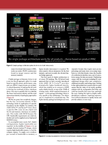
Figure 3: Sample package architecture options for die-to-die chiplet interconnects.
             omni-directional interconnect (ODI),   higher density interconnect is required. We   expensive because they require more precise
             wafer-on-wafer (WoW) architecture   chose passive silicon interposers for the first   patterning and many more processing steps;
             found in image sensors and the   instance, and most recently, the elevated fan-  however, with that density comes the benefits
             memory markets.               out bridge approach.               of a reduction in interface area, and of course,
                                             The holy grail of chiplet architecture is   lower energy for data movement. Chipletizing
          Chiplet package architecture choice is not   of course 3D stacking. The 3D hybrid bond   comes with the overheads including IO area,
        a one size fits all approach, rather it is made   approach that we have recently introduced   additional design effort and complexity,
        based on specific power, performance, area,   with AMD 3D V-Cache™ provides   additional assembly and testing steps. Getting
        and cost (PPAC) requirements per product.   dramatically higher bandwidth density,   to the right architecture requires that we must
        A critical dimension of making this all work   which has enabled us to connect a 64MB   ensure that the value of our newly modular
        is driving the overhead of those interfaces   cache chiplet directly on top of the 32MB of   solution with its configuration flexibility and
        down. One way to quantify this is to tabulate   existing cache, which required thousands of   yield has benefits that more than outweigh
        the linear interconnect density and the areal   signals—so the package technology choice is   the costs. Getting this right is a highly multi-
        interconnect density of packaging approaches   very specific to the architecture. The choice   disciplinary endeavor, requiring engineers
        (Figure 4).                        can be visualized in a simplified way. The   from different domains to rapidly iterate and
          MCMs are great, low-complexity designs,   higher density package technologies are more   provide solutions in new ways.
        but the low connection density of this
        technology limits its applications to specific
        boundaries for the chiplets. For instance, the
        AMD EPYC™ and Ryzen™ lines chose
        to put the CPU cores on one chiplet and
        the IO and memory interfaces on another
        one. This works with MCM because the
        CPU bandwidth requirements are relatively
        modest and can be supplied across highspeed
        SERDES routes.
          To accomplish more exotic SoC chiplet
        configurations, higher bandwidths are
        required. In the middle of Figure 4 is an
        example Radeon Instinct™ design, which
        requires high-bandwidth memory to feed the
        compute engines. To supply over a terabyte
        per second of bandwidth to memory, a
                                           Figure 4: Improving key parameters that drive high-performance computing forward.

                                                                                                             15
                                                               Chip Scale Review   May  •  June  •  2022   [ChipScaleReview.com]  15

