Page 10 - Chip Scale Review_May June_2022-digital
P. 10
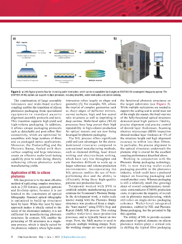
Figure 3: a) (left) Typical process flow for imprinting wafer-level optics, which can be accomplished by b) (right) an EVG7300 UV nanoimprint lithography system. The
        EVG7300 UV-NIL system can support multiple processes, including SmartNIL, wafer-level optics and device stacking.
          The combination of large assembly   interaction relies largely on shape and   the functional photonic structures on
        tolerances and wide-band surface   geometry [3]. For example, NIL allows   the target substrates (see Figure 3).
        coupling enables the transition of silicon   the imprint of complex geometries such   While multiple replications are needed to
        photonics packaging from specialized   as sharp edges of deflector mirrors,   support the scaling and to avoid wear out
        e q u i p m e n t t o s t a n d a r d p a s s i ve   curved surfaces, high and low aspect   of the single die master, the final imprints
        alignment assembly protocols and tools.   ratio structures as well as imprinting in   of the fully-functional optical structures
        This transition supports high-yield and   deep cavities. Wafer-level optics (WLO)   demonstrated high pattern fidelity,
        high-volume packaging. In addition,   processes have long proven their high   precise alignment and precise control
        it allows unique packaging protocols   repeatability in high-volume production   of desired layer thicknesses. Scanning
        such as detachable and post-reflow fiber   for optical sensors and are now being   electron microscope (SEM) inspection
        connectivity, which are optimized for   leveraged for photonic packaging.  showed residual layer thickness at <1% of
        assemblies with large numbers of fibers   The NIL process offers significant   the structure height and high alignment
        and co-packaged optics applications.   yield and cost advantages for the above-  accuracy to within less than 500nm.
        Moreover, the PhotonicPlug and the   mentioned  structures compared to   In particular, the precise alignment to
        Photonic Bump, fueled with their   conventional manufacturing methods,   the optical structures underneath the
        surface coupling and large tolerances,   such as diamond drilling, laser direct   photonic chip is crucial for the excellent
        create an effective wafer-level testing   writing and electron-beam writing,   coupling performance described above.
        capability prior to wafer dicing, thereby   which have very low throughput and   Working in conjunction with the
        enhancing silicon photonics wafer   are therefore difficult to scale up to   Photonic Bump packaging technology,
        manufacturing yields.              larger substrates and volume-production   N I L  is  now  m a k i ng  wafe r- scale
                                           environ ments. Incor porating the   packaging possible in the photonics
        Application of NIL to silicon      NIL process enables the use of best-  industry, which could have a profound
        photonics                          performing dies and the ability to   impact on lowering packaging and
          NIL has proven to be the most effective   efficiently bring these high-quality   overall product costs. Whereas packaging
        method of replicating complex structures,   patterns into production lines.  is still a relatively small (but growing)
        such as 2.5D features, grayscale patterns   Teramount worked with EVG to   share of overall complementary metal-
        and freeform optics, because it is not   establish suitable manufacturing process   oxide semiconductor (CMOS) production
        limited to the constraints of optical   solutions for Teramount’s Photonic Bump.   costs, it represents the majority of overall
        lithography. Standard optical lithography   In the development work, a wafer-scale   cost in photonics manufacturing, which
        is optimized to build  up structures   master stamp with the Photonic Bump   still relies on single-device packaging
        layer by layer. While this layer by layer   structures was produced from a single-  schemes. Wafer-level i nteg rated
        approach makes it ideally suited to the   die “hard master” using EVG’s Step and   photonics, enabled by NIL and Photonic
        needs of the electronics industry, it is not   Repeat (S&R) NIL process. This scaling   Bump packaging, has the potential to flip
        sufficient for manufacturing photonic   enables wafer-level mass-production   this equation.
        structures. In contrast, NIL enables the   processes, and is typically based on two   The ability of NIL to provide accurate
        patterning of 3D structures in a single-  steps. First, the S&R master is used to   placement of optical elements on silicon
        step process, which is ideally suited for   replicate multiple working stamps. Next,   photonics wafers plays a critical role
        the photonics industry where light-matter   the working stamps are used to imprint   in shifting the typical fiber packaging

        8 8  Chip Scale Review   May  •  June  •  2022   [ChipScaleReview.com]

