Page 8 - Chip Scale Review_May June_2022-digital
P. 8
TECHNOLOGY TRENDS


                           Scalable silicon photonics packaging using


                           optical bump nanoimprint lithography


                           By Hesham Taha [Teramount Ltd] and Martin Eibelhuber  [EV Group]

        S        ilicon photonics has emerged   limiting factor in existing silicon photonics


                                             Fiber-to-chip assembly is the main
                 as a promising platform for
                 supporting the ever-growing
                                           fiber bonding on a photonic chip with
                 demand for high-speed data   packaging solutions, which use direct
        transfer, low-power consumption and low   adhesives through active alignment or
        latency, which are required for the next   specialized high-precision alignment
        generations of data centers, advanced   equipment. These are limited in their
        computing, and 5G/6G networks and   volume manufacturability, scalability to
        sensors. The silicon photonics market   large numbers of fibers, compatibility
        has expanded significantly in the last few   with packaging processes such as reflow
        years and is expected to grow at a 26.8%   requirements, and integration with
        compound annual growth rate (CAGR)   electronics packaging. The essence of
        over the next five years [1]. While wafer   the problem is related to geometrical
        manufacturing capabilities for silicon   constraints of tight assembly tolerances   Figure 1: Photonic Bump wafer-level imprint on a
        photonics are well advanced through the use   when packaging single-mode fibers with   silicon photonics wafer at accurate placement relative
        of standard semiconductor mass-production   silicon or nitride waveguide channels   to waveguide channel.
        processes and existing infrastructure,   on a photonic chip, as well as related to
        silicon photonics packaging and testing are   the complex side-coupling geometry.   Photonic Bump elements provide unique
        still behind and lack production scalability,   These impose critical obstacles for silicon   optical coupling functionalities that include:
        which limits wider deployment of silicon   photonics to be able to be applied to wider   1) a vertical beam deflection to enable wide-
        photonics. Photonic Bump technology, a   applications such as co-packaged optics in   band surface coupling as a replacement for
        new wafer-level implementation of optical   ethernet switches, advanced computing and   the complicated side-coupling geometry;
        elements for scalable packaging and testing   future chip-to-chip optical connectivity.   and 2) a spot size conversion for mode
        capabilities, is presented in this article.   Teramount and EV Group have   matching between single-mode fiber and
        The Photonic Bump is an equivalent of   collaborated to adopt wafer-level   the chip’s waveguide (see Figure 1). In
        electrical solder bumps and has the potential   optics technologies in order to enhance   addition, Photonic Bumps are used to
        to align silicon photonics with standard   silicon photonics packaging processes.   enable the “self-aligning optics” scheme
        semiconductor wafer manufacturing   Under this collaboration, nanoimprint   when connected with the Teramount
        and packaging lines, thereby bridging   lithography (NIL) has been used for   PhotonicPlug fiber connector [2], which
        the gap in silicon photonics toward   wafer-level implementation of Photonic   enables fiber-chip assembly tolerances of
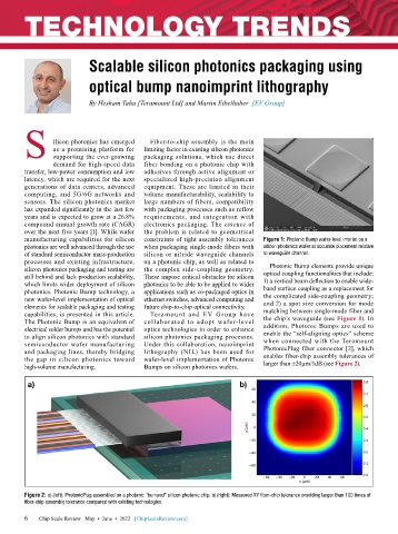
        high-volume manufacturing.         Bumps on silicon photonics wafers.  larger than ±20µm/1dB (see Figure 2).


        Figure 2: a) (left): PhotonicPlug assembled on a photonic “bumped” silicon photonic chip. b) (right): Measured XY fiber-chip tolerance providing larger than 100 times of
        fiber-chip assembly tolerance compared with existing technologies.

        6 6  Chip Scale Review   May  •  June  •  2022   [ChipScaleReview.com]

