Page 45 - ChipScale_Jul-Aug_2020-Digital
P. 45
System in package: a way forward for system integration


        By Favier Shoo, Santosh Kumar  [Yole Développement (Yole)]
        W            i t h a d v a n c e d n o d e   however, expensive, with low volume and   inside a mobile phone, digital music


                     scaling over the past
                                           that did not make it scalable.
                     decades, the resulting   low yield and with a tailored supply chain   player, etc. Dies containing integrated
                                                                              circuits may be stacked vertically on a
        semiconductors were expected to be more   SiP, as we know it today, emerged   substrate. They are connected internally
        cost effective, dissipate less power, and   during the 2000s, driven by mobile   by fine wires bonded to the package.
        have higher performance. Consequently,   a p pl ic at ion s’ f u nc t ion a l it y a nd   Alternatively, with flip-chip technology,
        the semiconductor industry was focused   miniaturization requirements. Volumes   solder bumps are used to join stacked
        mainly on how to produce all the   exploded because of the adoption of   chips together. SiPs are similar to SoCs,
        components that make up a system on a   various SiPs (but mainly radio frequency   but less tightly integrated, and are not on
        single chip, i.e., a system on chip (SoC)   [RF] applications) by mobile outsourced   a single semiconductor die.
        platform. In this megatrend-driven era,   semiconductor assembly and test suppliers   SiP dies can be stacked vertically
        however, more devices are starting to   (OSATS), who emerged as key assemblers.  or tiled horizontally, unlike less-
        rely on integrating separate components   The  SiP  business migrated from   dense MCMs in which dies are placed
        into a single system. Not all functions   integrated device manufacturers (IDMs)   horizontally on a carrier. In SiPs, the dies
        in a system need equivalent high-end   to OSATS where the supply chain is   are connected with standard off-chip wire
        performance, it is only by integrating   relatively more mature than that used for   bonds or solder bumps, unlike slightly
        components with the right value in the   MCMs. SiP integrates different chips   denser three-dimensional integrated
        package that the cost can be lowered   and discrete components, as well as 3D   circuits in which stacked silicon dies are
        and optimal price points achieved. As   chip stacking of either packaged chips or   connected by conductors running through
        a result, SoC has started to lose its   bare chips (i.e., wide-bandwidth memory   the die.
        appeal as a cost-efficient option for   cubes and memory on logic with through-  Most SiPs that went into high-
        functional integration. Instead, system   silicon vias [TSVs]) side-by-side on a   volume  manufacturing  (HVM)  over
        in package (SiP) opens a new door for a   common (either silicon, ceramic, or   the last decade are laminated MCM (or
        near boundless range of systems to be   organic) substrate to form a system or   MCM-L) for low-end applications like
        integrated into a package.         subsystem for smartphones, tablets, high-  smartphones, tablets, smartwatches,
          In the personal computer (PC) era   end networking servers, and computer   medical, wearable electronics, gaming
        of the 1980s, multi-chip modules   applications. SiP technology encompasses   systems, and consumer products.
        (MCMs) (a similar concept to SiP at   both horizontal and vertical integration.  I nter net  of T hi ngs  (IoT) -related
        the module-level—SiP is also referred   As noted above, SiPs are several   products, i.e., smart homes, smart
        to as “vertical MCM” or “3D MCM”)   integrated circuits enclosed in a single-  energy, and smart industrial automation,
        were first developed by IBM to package   chip carrier package. The SiP performs   were also involved. For these types
        processors for data centers and enterprise   all, or most, of the functions of an   of applications, the SiPs usually have
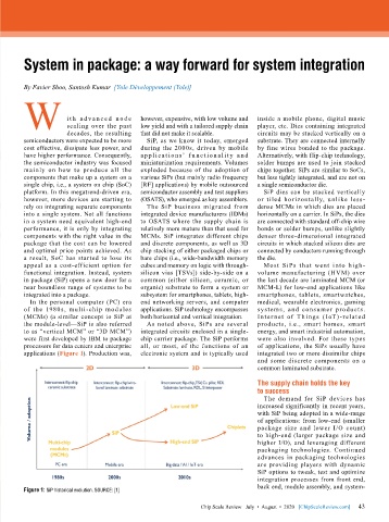
        applications (Figure 1). Production was,   electronic system and is typically used   integrated two or more dissimilar chips
                                                                              and some discrete components on a
                                                                              common laminated substrate.

                                                                              The supply chain holds the key
                                                                              to success
                                                                                The demand for SiP devices has
                                                                              increased significantly in recent years,
                                                                              with SiP being adopted in a wide-range
                                                                              of applications: from low-end (smaller
                                                                              package size and lower I/O count)
                                                                              to high-end (larger package size and
                                                                              higher I/O), and leveraging different
                                                                              packaging technologies. Continued
                                                                              advances in packaging technologies
                                                                              are providing players with dynamic
                                                                              SiP options to tweak, test and optimize
                                                                              integration processes from front end,
                                                                              back end, module assembly, and system-
        Figure 1: SiP historical evolution. SOURCE: [1]

                                                                                                             43
                                                             Chip Scale Review   July  •  August  •  2020   [ChipScaleReview.com]  43

