Page 47 - Chip Scale Review_November-December_2023-digital
P. 47
®
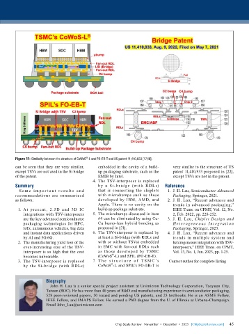
        Figure 11: Similarity between the structure of CoWoS -L and FO-EB-T and US patent 11,410,933 [17,19].
        can be seen that they are very similar,   embedded in the cavity of a build-  very similar to the structure of US
        except TSVs are not used in the Si bridge   up packaging substrate, such as the   patent 11,410,933 proposed in [22],
        of the patent.                         EMIB by Intel.                     except TSVs are not in the patent.
                                             4.  The TSV-interposer is replaced
        Summary                                by a Si- b r id ge (w it h R DL s)   Reference
          S o m e  i m p o r t a n t  r e s u l t s  a n d   that is connecting the chiplets   1.  J. H. Lau, Semiconductor Advanced
        recommendations are  summarized        with microbumps such as those      Packaging, Springer, 2021.
        as follows:                            developed  by  IBM,  AMD,  and   2.  J. H. Lau, “Recent advances and
                                               Apple. There is no cavity on the   trends in advanced packaging,”
          1.  At  pre se nt ,  2.5D  a nd  3D  IC   build-up package substrate.   IEEE Trans. on CPMT, Vol. 12, No.
            integrations with TSV-interposers   5.  The microbumps discussed in item   2, Feb. 2022, pp. 228-252.
            are the key advanced semiconductor   #4 can be eliminated by using Cu-  3.  J. H. Lau,  Chiplet Design and
            packaging technologies for HPC,    Cu bump-less hybrid bonding as     H e t e r o g e n e o u s  I n t e g ra t i o n
            IoTs, autonomous vehicles, big data   proposed in [21].               Packaging, Springer, 2023.
            and instant data applications driven   6.  The TSV-interposer is replaced by   4.  J. H. Lau, “Recent advances and
            by AI and 5G/6G.                   at least a Si-bridge (with RDLs and   trends  in  multiple  system  and
          2.  The manufacturing yield loss of the   with or without TSVs) embedded   heterogeneous integration with TSV-
            ever-increasing size of the TSV-   in EMC with fan-out RDLs such      interposers,” IEEE Trans. on CPMT,
            interposer is so high that the cost   as those developed by TSMC      Vol. 13, No. 1, Jan. 2023, pp. 1-25.
                                                      ®
            becomes unbearable.                (CoWoS -L) and SPIL (FO-EB-T).
          3.  The TSV-interposer is replaced   7.  T h e  s t r u c t u r e  o f  T SMC’s   Contact author for complete listing
                                                     ®
            by the Si-bridge (with RDLs)       CoWoS -L and SPIL’s FO-EB-T is


                       Biography
                         John H. Lau is a senior special project assistant at Unimicron Technology Corporation, Taoyuan City,
                       Taiwan (ROC). He has more than 40 years of R&D and manufacturing experience in semiconductor packaging,
                       528 peer-reviewed papers, 50 issued and pending US patents, and 23 textbooks. He is an ASME Fellow,
                       IEEE Fellow, and IMAPS Fellow. He earned a PhD degree from the U. of Illinois at Urbana-Champaign.
                       Email John_Lau@unimicron.com


                                                                                                             45
                                                       Chip Scale Review   November  •  December  •  2023   [ChipScaleReview.com]  45

