Page 43 - Chip Scale Review_May June_2023-digital
P. 43
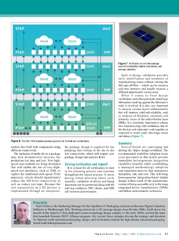
Figure 7: Verification of complete package
                                                                              assemblies including chiplets, interposers, and
                                                                              package substrate.
                                                                                Such in-design validation provides
                                                                              early identification and resolution of
                                                                              manufacturing issues without running the
                                                                              full sign-off flow – which can be resource
                                                                              and time intensive and usually requires a
                                                                              different department’s involvement.
                                                                                W hen it comes to f inal desig n
                                                                              verification, more than just mask metal layer
                                                                              fabrication checking against the fabricator’s
                                                                              rules is involved. It is also very important
                                                                              to analyze various layout enhancements
                                                                              that will improve yield and reliability, such
                                                                              as analysis of thickness variations and
                                                                              planarity issues of the redistribution layer
                                                                              (RDL). It is extremely important to release
                                                                              into manufacturing with confidence that all
                                                                              the devices and substrates work together as
                                                                              expected to avoid costly late-stage errors
                                                                              and delays (Figure 7).

        Figure 6: The IEEE 1838 standard provides guidance for 3D multi-die architectures.
                                                                              Summary
        stacked dies built with components using   the package design is required for the   Several factors are converging and
        different vendor tools.            planning and routing of the die-to-die   driving the chiplet design revolution. The
          The inclusion of multi-die in a package   test connectivity, which will require new   recommended workflow adoption focus
        may also dramatically increase the   package design and analysis flows.  areas presented in this article provide
        production test time and cost. New high-                              immediate heterogeneous integration
        speed scan methods are being developed   Driving verification and signoff  capability benefits while establishing
        that will enable the use of very high-  It is critical for all verification to start   a managed methodology adoption
        speed test interfaces, such as XSR, to   in the planning process and continue   and migration process that minimizes
        replace the traditional slow-speed JTAG   throughout the layout process. It starts   disruption, risk, and cost. This will bring
        approach, which should significantly   during initial planning where early   heterogeneous integration-based chiplet
        reduce the SiP-level connectivity as   assembly validation of device and bump   design within reach of the mainstream,
        well as reduce test time. Because the   placement can be performed along with IO   instead of being accessible only to the mega
        test connectivity in 2.5D devices is   pad ring validation, ERC checks, and ESD   integrated device manufacturers (IDMs)
        implemented through an interposer,   cell insertion determination.    and fabless semiconductor companies.


                       Biography
                         Keith Felton is the Marketing Manager for the Xpedition IC Packaging solutions at Siemens Digital Industries
                       Software in Marlborough, MA. Working extensively in IC package design since the late 1980s, Keith drove the
                       launch of the industry’s first dedicated system-in-package design solution in the early 2000s and led the team
                       that launched Siemens OSAT Alliance program. His current focus includes driving the strategy and direction
                       for Siemens multi-substrate prototyping, design, and verification solution for high-density advanced packaging.
                       Email keith.felton@siemens.com


                                                                                                             41
                                                               Chip Scale Review   May  •  June  •  2023   [ChipScaleReview.com]  41

