Page 40 - Chip Scale Review_May June_2023-digital
P. 40
1.  C h i p l e t d e s i g n k i t s (C D K )
                                                                                  provide a model of the chiplet for
                                                                                  implementation and integration.
                                                                                  A CDK can include interface
                                                                                  protocols, IO models, automatic
                                                                                  test equipment (ATE) test methods,
                                                                                  power characteristics, and thermal
                                                                                  models such as boundary condition
                                                                                  independent reduced order model
                                                                                  (BCI-ROM).
                                                                                2.  Heterogeneous planning and co-
                                                                                  optimization should use a complete
                                                                                  3D digital model (aka digital twin) of
                                                                                  the entire device assembly that drives
                                                                                  all downstream aspects of design,
                                                                                  analysis, and verification, maintaining
                                                                                  a continuous digital thread.
                                                                                3.  Physical verification at every level
                                                                                  of 3D assembly, from the substrate
                                                                                  layer through design rule checks
        Figure 2: Example of smart HBM channel replication.                       to assembly-level layout-versus-
        greater designer effort and the need to   Clearly, advanced packaging design   schematic are important.
        draw upon more specialized expertise,   workflows need to be improved to meet   4.  Multi-domain testing starting with
        which  increases  design  cycle  time.   the  needs  of  companies  creating  HI   the individual die and continuing
        One way to attack this is by deploying   platforms—ideally in a manner that   with die-to-die and across the entire
        multiple designers concurrently on the   doesn’t require expensive tool add-ons   package assembly is also important.
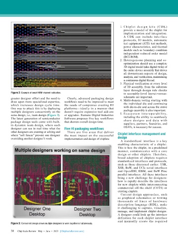
        same design, i.e., team design (Figure 3).   or upgrades. Siemens Digital Industries   5.  Ec o s yst e m  i nt er op er a bi lit y,
        The latest generation of semiconductor   Software proposes five key workflows   including the ability to seamlessly
        package design tools come with built-  that shorten overall design time.  sha re desig n s a nd d at a w it h
        in dynamic team design, where each                                        suppliers, partners, foundries, and
        designer can see in real time what the   Five HI packaging workflows      OSATs, is necessary for success.
        other designers are creating or editing and   There  are  five  areas  that  deliver
        where “soft fences” prevent one designer   the most impact on the successful   Chiplet interface management and
        overriding another designer’s work.  implementation and design of chiplets:  design
                                                                                A  standardized  interface  is  a  key
                                                                              enabling characteristic of a chiplet.
                                                                              This is how the chiplet, in a predefined
                                                                              manner, communicates with a core
                                                                              design or other chiplets. Therefore,
                                                                              broad adoption of chiplets requires
                                                                              standardized interfaces and protocols,
                                                                              such as those discussed earlier: USR,
                                                                              XSR, BoW, and UCIe serial interfaces
                                                                              and OpenHBI, HBM, and BoW Fine
                                                                              parallel interfaces. All these interfaces
                                                                              bring a new challenge for designers:
                                                                              how to rapidly describe the interfaces
                                                                              for new chiplets while interconnecting
                                                                              commercial off-the-shelf (COTS) or
                                                                              existing chiplets.
                                                                                Current design approaches, such
                                                                              as graphical schematics or writing
                                                                              t hou s a nd s of l i ne s of h a rd wa r e
                                                                              description  language  (HDL),  make
                                                                              it challenging to capture, visualize,
                                                                              manage, and implement chiplet designs.
                                                                              A designer could look up the interface
                                                                              definition for each chiplet interface
                                                                              and manually create the required
        Figure 3: Concurrent design allows multiple designers to work together simultaneously.

        38   Chip Scale Review   May  •  June  •  2023   [ChipScaleReview.com]
        38

