Page 41 - Chip Scale Review_May June_2023-digital
P. 41
connectivity in accordance with the
        specification, then define electrical
        constraints to ensure correct package
        design. But this is a lot of manual work
        and introduces the risk of human-
        generated mistakes that might not be
        easy to catch early in the design process.
        To avoid this risk, we will introduce a
        novel concept: interface-based design.
        Automating interface-based design
          Interface-based design (IBD) is an
        exciting new approach to capturing,
        designing, and managing large numbers
        of complex interfaces that interconnect
        multiple chiplets. Because the chiplet
        has a known formal interface, the
        interface description can become part of
        the chiplet part model. When a designer
        places an instance of this chiplet,
        everything related to the interface is
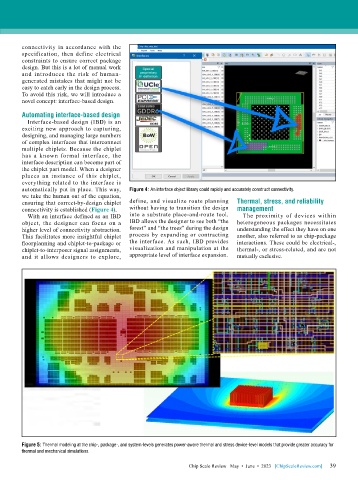
        automatically put in place. This way,   Figure 4: An interface object library could rapidly and accurately construct connectivity.
        we take the human out of the equation,
        ensuring that correct-by-design chiplet   define, and visualize route planning   Thermal, stress, and reliability
        connectivity is established (Figure 4).  without having to transition the design   management
          With an interface defined as an IBD   into a substrate place-and-route tool.   The  proximity  of  devices  within
        object,  the  designer  can  focus  on  a   IBD allows the designer to see both “the   heterogeneous packages necessitates
        higher level of connectivity abstraction.   forest” and “the trees” during the design   understanding the effect they have on one
        This facilitates more insightful chiplet   process by expanding or contracting   another, also referred to as chip-package
        floorplanning and chiplet-to-package or   the interface. As such, IBD provides   interactions. These could be electrical-,
        chiplet-to-interposer signal assignments,   visualization and manipulation at the   thermal-, or stress-related, and are not
        and it allows designers to explore,   appropriate level of interface expansion.  mutually exclusive.


        Figure 5: Thermal modeling at the chip-, package-, and system-levels generates power-aware thermal and stress device-level models that provide greater accuracy for
        thermal and mechanical simulations.

                                                                                                             39
                                                               Chip Scale Review   May  •  June  •  2023   [ChipScaleReview.com]  39

