Page 39 - Chip Scale Review_May June_2023-digital
P. 39
Slipping IC package design schedules and


        what to do about it


        By Keith Felton  [Siemens Digital Industries Software]
        S        everal  factors  are  causing


                 advanced packaging design
                 schedules to slip to a perilous
        degree. This article enumerates five
        factors that cause increasing design
        cycles and presents five workflows to get
        around them and get IC packaging design
        work back on track.

        Designs are getting more complex
          First, as with all semiconductor designs,
        increasing complexity continues to create
        new challenges for package design,
        verification, and modeling. Packages
        are now heterogeneous integration (HI)
        platforms and are no longer simply a
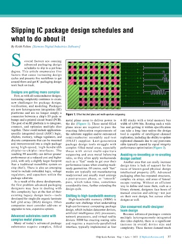
        connector between a chip’s IO pads or   Figure 1: Offset hatched plans and multi-aperture outgassing.
        bumps and a printed circuit board (PCB).   metal plane areas to deliver power to   4-HI stacks with a total memory bus
        The goal of an HI platform is to integrate,   the die (Figure 1). These metal-filled   width of 4,096 bits. Routing such a wide
        connect, and optimize multiple dies   plane areas are required to pass the   bus and getting it within specification
        together. These could include application-  exacting fabrication requirements of   can take a long time unless the design
        specific integrated circuit (ASIC) logic,   the substrate supplier and/or outsourced   tool is capable of intelligent channel
        chiplets, memory, voltage regulators, and   semiconductor assembly and test   replication, including the ability to update
        discrete components that can be mounted   (OSAT) supplier. Last-generation   replicated channels due to any post-route
        and interconnected into a single package   package design tools struggle with   edits typically caused by signal integrity
        using high-speed, high-bandwidth   complex filled metal areas, especially   performance optimization (Figure 2).
        chiplet-to-chiplet interfaces. The   t hose  w it h  st r ict  mult i-aper t u re
        resulting HI assembly can deliver greater   outgassing and area metal balancing   Avoiding re-inventing or re-creating
        performance at a reduced cost and higher   rules, so they often apply workarounds   design content
        yield, with only a slightly larger footprint   such as a “fast” mode to get over their   Another area that can easily increase
        than a traditional monolithic system on   performance issues when creating mask-  design time is lack of support for the
        chip (SoC). There is also an emerging   ready geometries. Of course, such “fast”   reuse of known-good physical design
        trend to include embedded logic, voltage   modes are typically not manufacturing   intellectual property (IP). Advanced
        regulators, and capacitors within the   ready/correct and usually must undergo   packaging often has repeated structures,
        package substrate.                 a post-process phase, or “smooth”   complex via arrays, and areas of fanout/
          As a result of the above developments,   pass, which takes time, sometimes   escape routing. Without an efficient
        the first problem advanced packaging   considerable time, further extending the   way to define and reuse them, such as a
        designers may face in dealing with   design cycle.                    library element, designers face hours of
        this complexity lays at the feet of their                             manual creation and editing—not just
        existing  legacy  design  tools—tools   Shifting to high-bandwidth memory  on their own design, but across other
        developed for single-die organic laminate   High-bandwidth memory (HBM) is   designs as well.
        ball grid array (BGA) designs. Often   another new challenge when undertaking
        companies must consider add-ons or   high-performance computing package   Use concurrent multi-designer
        upgrades to new, expensive options.  design, which includes datacenter devices,   team design
                                           artificial intelligence (AI) processors,   Because advanced packages contain
        Advanced substrates come with      network processors, and virtual reality   multiple  heterogeneously-integrated
        complex metal planes               devices. HBM has exacting routing rules   dies (aka chiplets), there is a significant
          Many of today’s advanced package   and requires a massively-parallelized   increase  in  overall  device  size  and
        substrates require complex, filled   interface, typically implemented as four   complexity. These factors demand much


                                                                                                             37
                                                               Chip Scale Review   May  •  June  •  2023   [ChipScaleReview.com]  37

