Page 17 - Chip Scale Review_May June_2023-digital
P. 17
TSV oxide etch-back optimization for the via-last


        integration scheme


        By Bhesetti S. S. Chandra Rao, Hemanth K. Cheemalamarri, Darshini Senthilkumar
        [Institute of Microelectronics, Agency for Science, Technology and Research (A*STAR)]
        T        hrough-silicon  via  (TSV)   scaling to enable higher integration


                 technology has become the key
                                           heterogeneous technologies [3,4].
                 driver for advanced electronic   densities along with the integration of
        packages such as those used in 3D stacking   The  use  of  TSVs  has  become  a
        and backside illuminated image (BSI)   prominent interconnect technology for
        sensor applications. Among the various   signal integrity through vertical stacking
        possible methods of integrating  TSVs such   [5-6]. There are several approaches for
        as via first, via middle and via last, the via-  TSV formation. The via-first approach
        last method has gained much attention. The   creates the TSVs before the front-end-of-
        via-last method helps reduce the impact   line (FEOL) and BEOL processes. The
        on back-end-of-line (BEOL) processing   via-middle approach carries out FEOL
        and does not require a TSV-reveal process   fabrication, followed by TSV and BEOL
        flow. However, the via-last process scheme   fabrications. The via-last approach [6]
        requires a more reliable TSV bottom-oxide   forms the TSVs after FEOL and BEOL
        etch-back process for making contact with   fabrications. In the via-after bonding
        the underneath interconnect layer. One   approach, vias are formed after bonding
        potential challenge with respect to the   either chip-to-wafer (C2W) schemes
        oxide etch-back process is in protecting the   or wafer-to-wafer (W2W) schemes.
        top corner of the TSV liner oxide to ensure   Depending on the integration scheme, the
        better electrical reliability. This challenge   via-last or via-after bonding is selected
        arises because the etch rate (ER) at the   for heterogeneous integration applications   Figure 1: a) Schematic of the oxide liner for the via-
        bottom of the via is much lower than at the   [7], like complementary metal-oxide   last integration approach; b) Effect on the TSV’s top-
        top corner of the TSV. This work focuses   semiconductor microelectromechanical   corner oxide, after oxide etch.
        on process methodology to increase the   systems (CMOS-MEMS). In the via-last   However, the bottom-oxide etch back
        bottom-oxide ER while reducing the TSV’s   approach, the oxide liner is deposited on   in the TSV is more challenging and
        top-corner oxide.                  the Si TSV immediately after TSV dry   requires a better-optimized process to
          The oxide etch-back process has   etching and wet cleaning.         obtain higher ER at the bottom of the
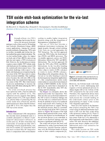
        been optimized with a fluorine-deficient   The Figure 1a schematic shows the   TSV compared to the top-corner oxide.
        regime with the addition of O 2 . The   typical post-oxide liner deposition. This   Therefore, this requirement drives more
        optimized process suggests that adding   liner not only acts as electrical isolation for   attention to the bottom-oxide etch-
        a slight amount of O 2  with argon-diluted   the TSV in terms of electrical leakage, but   back process for a smooth landing on
        C 4 F 8  plasma helps in protecting the top   will also help as a contamination barrier   the  underneath  contact  prior  to  the
        corner oxide more effectively and the   for the Si substrate in terms of re-sputtered   electroplating of copper in the via-last
        optimized process shows that the bottom-  metal underneath while landing on the   TSV integration approaches.`
        oxide ER is 20 to 30% higher than the   metal pad (aluminum or copper). During   There are a few reports in the literature
        TSV top-corner erosion.            the etch-back process, there is a potential   that propose protecting the TSV’s top
                                           issue of losing oxide at the TSV’s corner (as   corner using an additional protection layer
        Introduction                       shown in Figure 1b) because of the high   such as SiN over the liner oxide along
          Three-dimensional (3D) integration   plasma sheath potential at the corner, which   with optimized etching [9-11]. There is
        has become more prominent and is a   receives the highest ion bombardment. If   another integration approach to mitigate
        credible alternative to Moore’s Law-  the etch-back process is not controlled, it   top-corner oxide loss is by depositing a
        inspired  interconnect  advances  in   results in an electrical leakage path and   thick hard-mask oxide deposition (>1.5µm)
        recent years [1]. It also overcomes the   becomes a significant yield loss [9-11].  before TSV etch. However, this additional
        constraints of system-on-chip (SoC)   The oxide etch process has been well   process step incurs a higher cost of TSV
        technology in terms of performance, cost,   understood by using fluorine-based etch   fabrication and is less attractive for
        and time to market [2]. It becomes more   chemistries; ionized fluorine radicals   integration adoption.
        and more evident that 3D integration   react with the Si-broken bonds of silicon   This  study  focuses  on  TSV  oxide
        works in conjunction with semiconductor   oxide to form volatile compounds [8].   liner etch-back process optimization


                                                                                                             15
                                                               Chip Scale Review   May  •  June  •  2023   [ChipScaleReview.com]  15

