Page 19 - Chip Scale Review_May June_2023-digital
P. 19
on improving the bottom oxide ERs while simultaneously   using a negative photoresist (PR) and pattern-transferred using a
        minimizing the top-corner oxide ER. The design of experiments   EUV stepper. A TSV pattern of 10µm (critical dimension [CD]) is
        (DOE) is designed by considering the variables that help in   etched to a depth of ~45μm using a standard multiplexed time etch
        thicker passivation and minimizing the free radicals for silicon   process in an inductively-coupled plasma (ICP) chamber. After the
        etching. C 4 F 8  gas is known for a higher passivation deposition   TSV etch, the remaining PR is stripped using a high-temperature
        rate when mixed with argon. Argon addition helps in increasing   O 2  plasma. Subsequently, the wafer was wet cleaned to remove the
        the electron temperature, which, in turn, increases the plasma   post-etch residues.
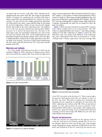
        density and results in the faster passivation rate. The addition   Figure 3 shows the post-etch and wet-cleaned TSV structure
        of O 2  to the C 4 F 8  increases passivation and thereafter further   with <40nm scallops and a near-vertical profile. The TSV
        increases in O 2  lowers the passivation rate. Because of the   wafers are deposited with a liner oxide of ~1μm using a plasma-
        high aspect ratio, the passivation deposition rate varies from   enhanced CVD (PE-CVD) process. Figure 4 shows the TSV
        the top to the bottom of the TSV—as the depth progresses, the   with liner oxide. The initial oxide thickness of the field (top),
        passivation transport mechanism changes from convective flow   top corner, and bottom of the TSV are measured at ~1.31μm,
        to diffusional flow, which results in more deposition at the TSV   ~0.86μm, and ~0.85μm, respectively. The step coverage ratio
        top than at the bottom. The process DOE targets minimizing
        the ratio of the oxide ERs between the TSV’s top corner and the
        bottom of the TSV.

        Materials and methods
          The wafer sample fabrication process flow is shown in the
        schematic (Figure 2). Wafer substrates of 300mm p-type (100) Si
        have been used for the current study. These wafers are spin coated


        Figure 2: Schematic of the process flow.


                                                             Figure 4: TSV structure after oxide liner deposition.

                                                             of the TSV top corner to the bottom is 1:1. This scenario makes
                                                             the process challenging if the ERs are similar or faster at
                                                             the TSV top corner. The DOE is conducted to determine the
                                                             optimum process conditions to minimize the top-corner ER
                                                             while enhancing the bottom-oxide ER. Process parameters
                                                             (argon, O 2 , C 4 F 8 , and pressure) are used to generate a full-
                                                             factorial DOE with the three center points. After etching, these
                                                             wafers were inspected using cross-sectional field-emission
                                                             scanning electron microscopy (FE-SEM) for post-etch liner
                                                             oxide thickness measurement.

                                                             Results and discussions
                                                               Fluorine radicals are responsible for the etching of the Si
                                                             in the dry etch process by forming volatile SiF 4  at even low
                                                             ion energies. However, in the case of SiO 2 , due to the stronger
                                                             energy threshold (an energy threshold of 799KJ/mol for the Si-O
                                                             bond, and 552KJ/mol for the Si-F bond [12]), the reaction can’t
        Figure 3: TSV structure prior to oxide liner deposition.

                                                                                                             17
                                                               Chip Scale Review   May  •  June  •  2023   [ChipScaleReview.com]  17

