Page 10 - Chip Scale Review_May June_2023-digital
P. 10
MCM rtMLF technology
          The following sections discuss various aspects of testing
        performed on the MCM rtMLF technology.
          Test vehicle and enhancement of small form factor.
        Information for the test vehicle is summarized in Table 1. Most
        descriptions are similar to a conventional QFN. Using this test
        vehicle, layout on the board was compared with two single QFN
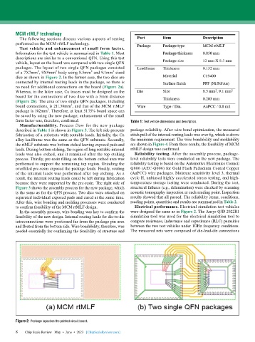
        packages. The layout of two single QFN packages consisted
                                                     2
                                           2
                           2
        of a 7X7mm , 9X9mm  body using 8.5mm  and 9.1mm  sized
                  2
        dice as shown in Figure 2. In the former case, the two dice are
        connected by internal routing leads in the package, so there is
        no need for additional connections on the board (Figure 2a).
        Whereas, in the latter case, Cu traces must be designed on the
        board for the connections of two dice with a 3mm distance
        (Figure 2b). The area of two single QFN packages, including
                                  2
        board connections, is 211.38mm , and that of the MCM rtMLF
        package is 102mm . Therefore, at least 51.75% board space can
                       2
        be saved by using the new package; enhancement of the small
        form factor was, therefore, confirmed.               Table 1: Test vehicle dimensions and description.
          Manufacturability. Process flow for the new package
        described in Table 1 is shown in Figure 3. The left side presents   package reliability. After wire bond optimization, the measured
        fabrication of a substrate with routable leads. Initially, the Cu   stitch pull of the internal routing leads was over 6g, which is above
        alloy leadframe was the same as the QFN substrate. Secondly,   the minimum requirement. The wire bondability and moldability
        the rtMLF substrate was bottom etched leaving exposed pads and   are shown in Figure 4. From these results, the feasibility of MCM
        leads. During bottom etching, the region of long routable internal   rtMLF design was confirmed.
        leads was also etched, and it remained after the top etching   Reliability testing. After the assembly process, package-
        process. Thirdly, pre-resin filling on the bottom etched area was   level reliability tests were conducted on the new package. The
        performed to support the remaining top region. Grinding the   reliability testing is based on the Automotive Electronics Council
        overfilled pre-resin exposed the package leads. Finally, routing   Q006 (AEC-Q006) for Gold Flash Palladium Coated Copper
        of the internal leads was performed after top etching. As a   (AuPCC) wire packages. Moisture sensitivity level 3, thermal
        result, the internal routing leads could be left during fabrication   cycle H, unbiased highly accelerated stress testing, and high-
        because they were supported by the pre-resin. The right side of   temperature storage testing were conducted. During the test,
        Figure 3 shows the assembly process for the new package, which   structural failures (e.g., delamination) were checked by scanning
        is the same as for the QFN process. Two dice were attached on   acoustic tomography inspection at each reading point. Inspection
        separated individual exposed pads and cured at the same time.   results showed that all passed. The reliability items, conditions,
        After this, wire bonding and molding processes were conducted   reading points, quantities and results are summarized in Table 2.
        to confirm feasibility of the MCM rtMLF design.        Electrical performance. Electrical simulation test vehicles
          In the assembly process, wire bonding was key to confirm the   were designed the same as in Figure 2. The Ansys Q3D 2022R1
        feasibility of the new design. Internal routing leads for die-to-die   simulation tool was used for the electrical simulation tool to
        interconnections were positioned far from the package pin area   compare resistance, inductance and capacitance (RLC) parasitics
        and floated from the bottom side. Wire bondability, therefore, was   between the two test vehicles under 1GHz frequency conditions.
        needed essentially for confirming the feasibility of structure and   The measured nets were composed of die-lead-die connections


        Figure 2: Package layout on the printed circuit board.

        8 8  Chip Scale Review   May  •  June  •  2023   [ChipScaleReview.com]

