Page 9 - Chip Scale Review Sep Oct_2022-digital
P. 9
State-of-the-art direct bonding    performance and energy efficiency to   can be achieved, with pitches ranging from
        technologies                       advanced 3D system-on-chip (SoC) devices.   10µm down to 1µm.
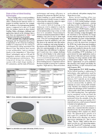
          Direct bonding offers several possibilities   Hybrid bonding is a good candidate for   Direct hybrid bonding offers two
        depending on the surface to be bonded: 1)   high-interconnect density because it enables   configurations of assembly: W2W and D2W
        either a homogeneous material surface is   connecting dies using tiny copper-to-copper   (Figure 1). W2W hybrid bonding is already
        bonded on another material, for example   connections, as opposed to bumps.  mature for imaging applications—starting
        III-V on silicon, or 2) a heterogeneous (hybrid)   To achieve hybrid bonding, a Cu   with Sony in 2016. It is characterized by the
        surface composed of a mix of Cu and   damascene level is adapted to reach the   alignment at wafer scale (Figure 2). With the
        SiO 2 , for instance, known as direct hybrid   applicable bonding specification after a   latest generation of W2W bonders, suppliers
        bonding. Stakes, advantages, challenges and   crucial planarization step is done on both   claim alignment capability below 50nm 3σ.
        applications depend on the technique that is   tiers to be assembled. Planarization by   The main advantage is high throughput, but
        used; these are summarized in Table 1 and   chemical mechanical planarization (CMP) is   the drawback is low flexibility for design
        explained in the following paragraphs.  definitely a key process step to ensure high   because bottom and top dies need to have the
          W2W and D2W direct hybrid bonding.   yield. Ultra-low nanotopography must be   same dimension. For more design flexibility,
        Packaging and 3D integration have grown   guaranteed from the millimeter scale (flat   hybrid bonding D2W is more suitable. This
        in importance as two of the key technology   die) down to the material scale (flat surface   process re-uses the know-how developed
        enablers to compensate for the slowing of   with low roughness) and going through to   for W2W, but it adds dicing and cleanliness
        two-dimensional scaling associated with   the micron scale (flat pattern). Enabling this   challenges. The known good die (KGD)
        Moore’s Law. Big players have moved   ultra-low nanotopography in the space of   concept can be applied to increase the overall
        to new architectures, such as chiplets,   the design rules with different Cu densities   product yield by selecting only good dies
        thanks to the integration of “More than   and Cu pad sizes was a unique challenge   before assembling. DTW technology is of
        Moore” technologies, such as 2.5D and 3D   that was solved thanks to the achievement   great interest for many applications such as
        integration, memory cubes, accelerators   of CMP process control of consumables   edge devices with more and more real-time
        and heterogeneous architectures. This   (slu r r y/pad /d ia mond d isk /recipe   computing of a large amount of data with
        integration brings key elements of   parameters). A precise alignment during the   a limited power budget. Other “More than
        success with a much larger number of    direct bonding process is required to achieve   Moore” applications are good candidates
        I/O connections, and the trade-off between   the electrical path by joining the Cu patterns   like photonics with imagers and display for
                                           together. High-density interconnections   design flexibility, or optic transceivers and
                                                                              radio frequency (RF).
                                                                                Heterogeneous III-V D2W bonding.
                                                                              While hybrid bonding is addressing Si
                                                                              technologies, other applications need the
                                                                              superior III-V materials’ properties (electron
                                                                              and hole mobilities, direct band gap).
                                                                              However, III-V materials are not available
                                                                              in large substrate diameters, thereby closing
                                                                              access to advanced fabs. In addition, raw
                                                                              materials are scarce, making bulk substrates
                                                                              costly. Therefore, new solutions are needed to
                                                                              combine the advantages of III-V materials on
                                                                              a silicon wafer, which refers to heterogeneous
                                                                              III-V D2W bonding here. Two approaches
                                                                              can be considered: on the one hand, the
                                                                              technology (laser cavity, for instance) is
        Table 1: Stakes, advantages, challenges and applications depend on each technique.
                                                                              performed before the assembly. It has the
                                                                              advantages of having good quality III-V
                                                                              materials and only a small amount of material
                                                                              is bonded at the right place [3].
                                                                                A second path can be considered in
                                                                              which only a material thin-film template is
                                                                              transferred onto the silicon platform, using
                                                                              direct bonding of III-V coupons on a silicon
                                                                              wafer. The epitaxial device growth, or at
                                                                              least a part of it, could then be done later
                                                                              on the silicon wafer, allowing very narrow
                                                                              inter-device shrinkage [4]—this is called
                                                                              “tiling.” This die “tiling” could be done on a
                                                                              sparse area but, in a very interesting manner,
                                                                              using the SmartCut™ technology, a large
                                                                              area could be covered within an industrial
        Figure 1: a) (left) W2W and b) (right) D2W bonding. SOURCE: CEA-Leti

                                                         Chip Scale Review   September  •  October  •  2022   [ChipScaleReview.com]  7 7

