Page 14 - Chip Scale Review Sep Oct_2022-digital
P. 14
bonding,” ECS Trans., vol. 3, no 6, p.
                                                                                   205, Oct. 2006.
                                                                                3.  B. Szelag, et al., “Advances on large-
                                                                                   scale integration CMOS-compatible
                                                                                   hybrid III-V/Si laser on 200mm
                                                                                   platform,” Smart Photonic and
                                                                                   Optoelectronic Integrated Circuits
                                                                                   XXI, Mar. 2019, vol. 10922, p.
                                                                                   109221O.
                                                                                4.  C. Besancon, et al., “AlGaInAs MQW
                                                                                   laser regrowth on heterogeneous InP-
                                                                                   on-SOI: performance for different
                                                                                   silicon cavity designs,” Optical Fiber
                                                                                   Comm. Conf. (OFC) 2021, p. W1B.1.
                                                                                5.  B. Ghyselen, et al., “Large-diameter
                                                                                   III-V on Si substrates by the SmartCut
                                                                                   Process: The 200mm InP film on
                                                                                   Si substrate example,” Phys. Status
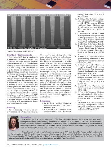
        Figure 8: TSV structures. SOURCE: CEA-Leti                                 Solidi A, vol. 219, no 4, p. 2100543,
        Benefits of TSVs for products      They enable the mixing of exotic        2022.
          Concerning D2W hybrid bonding, it   material and/or different technologies   6.  A. Jouve, et al., “Die-to-wafer direct
        is important to mention the role of TSVs   in one place for performance, design   hybrid bonding demonstration with
        (Figure 8). By nature, systems featuring   flexibility or heterogeneity. A wide   high alignment accuracy and electrical
        hybrid bonded types of interconnections   range of direct bonding processes   yields,” 3DIC, 2019.
        will require an access to embedded metal   meet several applications’ needs, from   7.  E. Bourjot, et al., “Toward a
        pads and, ideally, in an array format to   substrate development to back-end   complete direct hybrid bonding
        keep the density for further layer or ball   3D interconnections, and the ability   D2W integration flow: known-good
        grid array (BGA) connections, for example.   to manage bonding mechanisms and   dies and die planarization modules
        An elegant way to access these contacts   integration. For 3D schemes, direct hybrid   development,” 3DIC, 2019.
        is the use of TSVs. Depending on the   bonding in W2W and D2W versions are   8.  E. Bourjot, et al., “Known-good dies
        targeted products, several types of vias   extremely attractive for increasing high-  strategies compatible with D2W direct
        could be envisioned. For three-layer types   density interconnection. D2W pushes the   hybrid bonding,” IEEE 71st Elec.
        of imaging devices [10], high-density TSVs   assets of hybrid bonding by adding design   Comp. and Tech. Conf. (ECTC), 2021,
        in the range of Ø1µm and 10µm depth will   flexibility and high yield. Challenges to   pp. 470–475.
        be employed for the inner strata, while for   manage the trade-off between throughput   9.  E. Bourjot, et al., “10µm and 5µm
        active-interposer types of modules [11],   and alignment performance. Several   die-to-wafer direct hybrid bonding,”
        TSV middle processes of Ø5µm to Ø10µm   process options are in development,   ESTC, 2022.
        and 50µm to 100µm depth will be preferred.   such as improved P&P speed and self-  10.  P. Vivet et al., “Advanced 3D design
        The effective coupling of appropriate TSV   assembly, where equipment suppliers play   and technologies for 3-layer Smart
        and hybrid bonding technologies appears   a critical role.                 Imager,”  Inter. Symp. on VLSI Tech.,
        as a strong leverage for the development                                   Systems and Appl. (VLSI-TSA), 2022,
        of products with unprecedented dense   References                          p. 1-2.
        interconnection architectures.       1.  D. Radisson, “Collage direct sur   11.  P. Coudrain, et al., “Active interposer
                                                surfaces structurées,” PhD Thesis,   technology for chiplet-based advanced
        Summary                                 Grenoble, 2014.                    3D system architectures,” IEEE 69th
          Direct bonding technologies are    2.  F. Rieutord, et al., “Rough surface   ECTC, May 2019, pp. 569-578.
        key enablers for 3D microelectronics.   adhesion mechanisms for wafer

                       Biographies
                         Emilie Bourjot is a Project Manager at CEA-Leti, Grenoble, France. Her current activities involve
                       developing advanced hybrid bonding schemes for 3D integration. Prior to joining CEA-Leti, she worked with
                       GlobalFoundries (Germany, USA) and within the IBM Alliance (USA) on the development of advanced FDSOI
                       technologies and sub-3nm nodes. She earned a MSc in Materials Physics from INSA Lyon (France) and a PhD
                       from Aix-Marseille U., France. Email emilie.bourjot@cea.fr

                         Frank Fournel is head of wafer bonding engineering at CEA-Leti, Grenoble, France, and a board member
          of the international ECS Wafer Bonding Symposium Conference, the International WaferBond Conference, and the Low
          Temperature Bonding 3D Conference. He has a Master’s in Materials Science from Ecole Supérieure de Physique et de Chimie
          Industrielle de la ville de Paris (ESPCI) in Materials Science, and a PhD from Grenoble U.


        12   Chip Scale Review   September  •  October  •  2022   [ChipScaleReview.com]
        12

