Page 13 - Chip Scale Review Sep Oct_2022-digital
P. 13
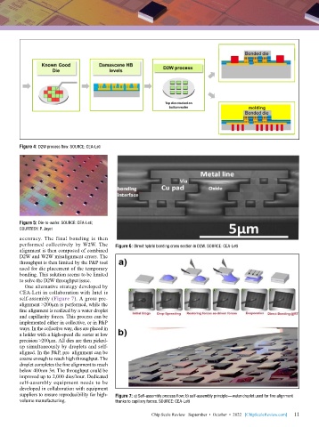
Figure 4: D2W process flow. SOURCE: CEA-Leti


        Figure 5: Die-to-wafer. SOURCE: CEA-Leti;
        COURTESY: P. Jayet
        accuracy. The final bonding is then
        performed collectively by W2W. The   Figure 6: Direct hybrid bonding cross section in D2W. SOURCE: CEA-Leti
        alignment is then composed of combined
        D2W and W2W misalignment errors. The
        throughput is then limited by the P&P tool
        used for die placement of the temporary
        bonding. This solution seems to be limited
        to solve the D2W throughput issue.
          One alternative strategy developed by
        CEA-Leti in collaboration with Intel is
        self-assembly (Figure 7). A gross pre-
        alignment >200µm is performed, while the
        fine alignment is realized by a water droplet
        and capillarity forces. This process can be
        implemented either in collective, or in P&P
        ways. In the collective way, dies are placed in
        a holder with a high-speed die sorter at low
        precision >200µm. All dies are then picked-
        up simultaneously by droplets and self-
        aligned. In the P&P, pre–alignment can be
        coarse enough to reach high throughput. The
        droplet completes the fine alignment to reach
        below 400nm 3σ. The throughput could be
        improved up to 2,000 dies/hour. Dedicated
        self-assembly equipment needs to be
        developed in collaboration with equipment
        suppliers to ensure reproducibility for high-  Figure 7: a) Self-assembly process flow; b) self-assembly principle—water droplet used for fine alignment
        volume manufacturing.              thanks to capillary forces. SOURCE: CEA-Leti

                                                         Chip Scale Review   September  •  October  •  2022   [ChipScaleReview.com]  11 11

