Page 11 - Chip Scale Review Sep Oct_2022-digital
P. 11
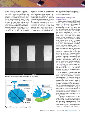
path (Figure 3). Using the SmartCut™   technology—it breaks the wafer-diameter   also opportunities because in that case, III-V
        technology involves first tiling III-V dies   ceiling and saves scarce material because   and Si devices are next to each other, which
        over a 200 or 300mm silicon substrate. This   only a thin layer is used rather than a bulk   facilitates the interconnects.
        creates a so-called pseudo-donor wafer paved   substrate. This type of tiling will be the key
        with dies several hundred microns thick.   technology to bring these III-V materials   Recent hybrid bonding D2W
        Second, this pseudo-donor is used to transfer   into high-volume manufacturing for display   improvements
        collectively thin layers (100-1,000nm) of   applications, for instance. Substrates tiled   The latest trends featured at ECTC 2022
        III-V dies on another silicon substrate using   with thin layers of III-V materials are then   showed a strong interest in hybrid bonding
        the SmartCut™ technology. The pseudo-  provided to foundries for further device   D2W. (Figures 4-5) [6–9]. Challenges
        donor substrate can be reused many times.   processing. In that case, III-V material   of direct hybrid bonding D2W remain in
        This work is underway jointly with Soitec [5].  is present at the front end of the device   performance, yield and cost, which are
          For applications using large III-V areas,   fabrication process. This brings challenges   driven by alignment capability, bonding
        the SmartCut™ tiling is a breakthrough   to co-process III-V materials and silicon, but   quality and throughput, respectively.
                                                                              Die bonder equipment is, therefore, a
                                                                              key piece for industrialization; it must
                                                                              meet class 1 cleanroom and accurate
                                                                              surface-bonding specifications. A fruitful
                                                                              collaboration between CEA-Leti and SET
                                                                              Corp. enabled emergence of a die bonder
                                                                              specifically designed for hybrid bonding
                                                                              D2W with alignment capability of 1µm
                                                                              3σ post bonding. It integrates a local clean
                                                                              environment, adaptation of robotics to
                                                                              avoid particulate contamination and precise
                                                                              alignment thanks to its optical alignment
                                                                              capability. Regarding yield, the cleaning
                                                                              post dicing was the other challenge. Regular
                                                                              sawing offers a simple way of dicing dies,
                                                                              but it has a high level of contamination. We
                                                                              have developed an efficient strategy for die
                                                                              cleaning. The combination of those skills
                                                                              enables demonstration of a high-yield level
                                                                              and an alignment capability below <1µm
                                                                              3σ (Figure 6), after bonding with high
                                                                              electrical yield [8-9]. However, ensuring
                                                                              a high throughput with a high bonding
                                                                              precision remains a big challenge from an
                                                                              economic perspective.
                                                                                Before explaining the different solutions
                                                                              under investigation, it is important to clarify
                                                                              some definitions of alignment. Machine
        Figure 2: Direct hybrid bonding cross section in W2W. SOURCE: CEA-Leti  intrinsic accuracy, die placement accuracy
                                                                              and die alignment post bonding are three
                                                                              components of global alignment. Machine
                                                                              intrinsic accuracy and die placement depend
                                                                              on optics, tool parameters and environment.
                                                                              The die integration characteristics and the
                                                                              alignment measurement method also play
                                                                              a role. Indeed, the best representation of
                                                                              a misalignment is a measurement at two
                                                                              extreme corners of the die. Therefore, the die
                                                                              alignment post bonding depends on all of
                                                                              those parameters.
                                                                                An accurate alignment takes a long
                                                                              time. Therefore, several approaches exist
                                                                              to increase throughput based on a pick
                                                                              and place (P&P) tool with increased speed
                                                                              or collective bonding. Here, collective
                                                                              bonding refers to pre-aligned dies with a
                                                                              temporary bonding and high alignment
        Figure 3: Schematic of the SmartCut™ tiling approach [5].

                                                         Chip Scale Review   September  •  October  •  2022   [ChipScaleReview.com]  9 9

