Page 37 - Chip Scale Review Sep Oct_2022-digital
P. 37
Extended electrical and thermal performance
          The f lexible lead configuration has enabled the MLF
        packaging technology to extend its capabilities for providing
        solutions in the power market. The Power QFN (PQFN) is
        a variant of the saw MLF technology that enables multiple
        customer exposed pads with multiple fused leads. Combined
        with the integration capabilities of copper (Cu) clips and heat
        slugs, the PQFN packaging solution has the thermal capability
        needed for power metal-oxide semiconductor field-effect
        transistor (MOSFET) designs while retaining the advantages
        of size (body thickness and body size). The split exposed pad
        capability is also a primary reason the MLF is finding success
        in the GaN market, especially for multi-die solutions where the
        gallium nitride (GaN) die and an application-specific integrated
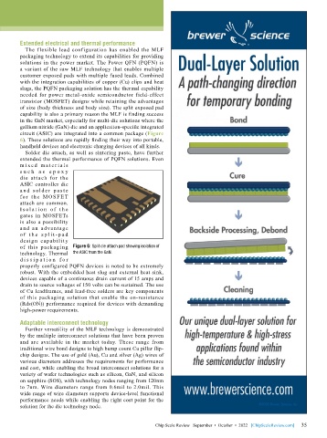
        circuit (ASIC) are integrated into a common package (Figure
        6). These solutions are rapidly finding their way into portable,
        handheld devices and electronic charging devices of all kinds.
          Solder die attach, as well as sintering paste, have further
        extended the thermal performance of PQFN solutions. Even
        m i x e d   m a t e r i a l s
        s u c h a s e p o x y
        die attach for the
        ASIC controller die
        a nd  s ol d e r  p a s t e
        fo r  t h e  MO SF E T
        attach are common.
        I s o l a t i o n o f t h e
        gates  in  MOSFETs
        is also a possibility
        and an advantage
        o f  t h e  s p l i t- p a d
        desig n capabilit y
        of this  packaging   Figure 6: Split die attach pad showing isolation of
        technology. Thermal   the ASIC from the GaN.
        d i s s i p a t i on   f o r
        properly configured PQFN devices is noted to be extremely
        robust. With the embedded heat slug and external heat sink,
        devices capable of a continuous drain current of 15 amps and
        drain to source voltages of 150 volts can be sustained. The use
        of Cu leadframes, and lead-free solders are key components
        of this packaging solution that enable the on-resistance
        (Rds(ON)) performance required for devices with demanding
        high-power requirements.

        Adaptable interconnect technology
          Further versatility of the MLF technology is demonstrated
        by the multiple interconnect solutions that have been proven
        and are available in the market today. These range from
        traditional wire bond designs to high bump count Cu pillar flip-
        chip designs. The use of gold (Au), Cu and silver (Ag) wires of
        various diameters addresses the requirements for performance
        and cost, while enabling the broad interconnect solutions for a
        variety of wafer technologies such as silicon, GaN, and silicon
        on sapphire (SOS), with technology nodes ranging from 120nm
        to 7nm. Wire diameters range from 0.6mil to 2.0mil. This
        wide range of wire diameters supports device-level functional
        performance needs while enabling the right cost point for the
        solution for the die technology node.


                                                                                                             35
                                                         Chip Scale Review   September  •  October  •  2022   [ChipScaleReview.com]  35

