Page 36 - Chip Scale Review Sep Oct_2022-digital
P. 36
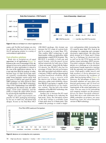
Figure 4: Body size and footprint are critical to application cost.

        count, and flexible lead designs are also   (DR-MLF) package, this format can   row configuration while increasing the
        key attributes that have led to the use of   increase the I/O count of a given body   I/O count by more than 30%. Seen as an
        this IC packaging solution in a variety of   size by as much as, or more than, 50%.   advantage in computing and consumer
        semiconductor applications.        This enables MLF technology to add   electronics applications, the ultra-fine
                                           functionality within an application while   pitch designs at 0.35mm and 0.30mm
        Cost-effective solutions           maintaining a small PCB footprint. The   can be a challenge for electrical test,
          Body size or footprint are of equal   DR-MLF is available in both saw and   as well as for the PCB layout and the
        importance to all applications (Figure 4).   punch formats, with the punch format   surface mount technology (SMT) process.
        Known as the cost of ownership (COO), the   utilized extensively for body sizes of 8mm   Fine-pitch contactor solutions for these
        amount of area on the printed circuit board   x 8mm and greater. Along with the higher   pitches are a challenge as is the electrical
        (PCB) of a given application is critical to   I/O density, the DR-MLF also has the   performance boards required to interface
        the cost of the application solution. So, it   advantage of better thermal performance   with the automatic test equipment (ATE)
        is not only how thick the package is today,   than other equivalent lead solutions such as   tester. High-quality solder stencils and
        but how large it is that can become more   a laminate CABGA and has demonstrated   high accuracy of device placement are
        of a priority consideration. Migration   excellent board-level reliability (BLR)   needed to minimize the incidence of
        paths from laminate carrier array ball   performance. Long a concern with   solder shorting during reflow (Figure 5).
        grid array (CABGA) and quad flat pack   the interior row of leads, data taken to   However, the advantages of these very
        (QFP) packages are often driven by these   determine solder joint reliability shows   fine-pitch solutions are seen where size,
        two advantages of the MLF technology.   that DR-MLF packaging is capable of the   thermal performance and I/O level are
        Other COO considerations seen with MLF   same BLR performance as the single-  justified by the critical and necessary
        packaging are the stencil costs, the solder   row versions. This has led to the recent   requirements of the actual application use
        usage, solder joint reliability, and the   adaptation of the DR-MLF technology into   cases. The use cases in the networking
        ability to inspect the solder reflow process   automotive applications.  and computer markets are the primary
        by monitoring the lead fillet formation.  Another way to increase the I/O count   drivers for these fine-pitch solutions.
          Higher pin count requirements are   of the MLF package is by reducing the   Hard disk drive and solid-state drive
        possible for MLF packaging technology   lead pitch. Today, the fine-pitch version   (SSD) controllers are primary use cases
        by the use of multi-row, interstitial lead   of the MLF design is available from   benefiting from this ultra-fine-pitch
        designs. Known as the Dual Row MLF   0.5mm pitch down to 0.30mm pitch. This   version of MLF technology.
                                           enables the package to retain a single-


        Figure 5: Illustration demonstrating fine-pitch progressions.

        34
        34   Chip Scale Review   September  •  October  •  2022   [ChipScaleReview.com]

