
Page 34 - Chip Scale Review Sep Oct_2022-digital
P. 34
Meeting cost and technology requirements using MLF/QFN
By Marc Mangrum [Amkor Technology, Inc.]
M icroLeadFrame (MLF)/ 0.30mm. Ultra-thin capability is also conditioning (HVAC) systems, medical
quad flat no-lead (QFN)
using both wire-bond and flip-chip
packaging technology possible down to less than 200µm devices, satellite systems, audio/
visual home electronics, and home and
is the fastest growing IC packaging interconnect solutions. The thinnest commercial appliances. In any identified
solution today. From a market segment IC packaging solution is the die itself electronic product, there is a 99.9%
perspective, MLF packaging solutions followed by wafer-level chip-scale chance a device utilizing QFN packaging
represent more than a 111B-unit market packaging (WLCSP) and then the MLF technology is in it. The wide use of this
for 2022 across five markets: automotive, over molded packaging technology. As packaging technology is not just about
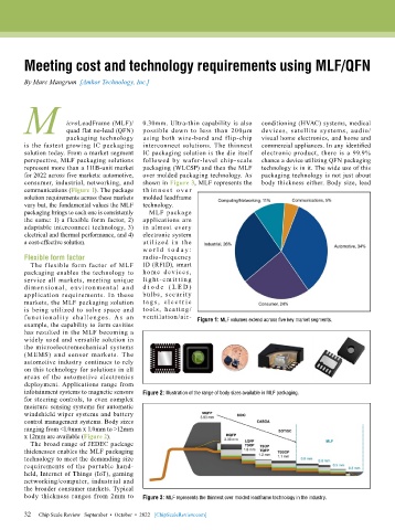
consumer, industrial, networking, and shown in Figure 3, MLF represents the body thickness either. Body size, lead
communications (Figure 1). The package t h i n n e s t o v e r
solution requirements across these markets molded leadframe
vary but, the fundamental values the MLF technology.
packaging brings to each one is consistently MLF package
the same: 1) a flexible form factor, 2) applications are
adaptable interconnect technology, 3) in almost every
electrical and thermal performance, and 4) electronic system
a cost-effective solution. utilized in the
w o r ld t o d ay :
Flexible form factor radio-frequency
The f lexible form factor of MLF ID (RFID), smart
packaging enables the technology to home dev ice s ,
service all markets, meeting unique l ight- e mit t i ng
di mensional, envi ron ment al and d i o d e ( L E D )
application requirements. In these bulbs, security
markets, the MLF packaging solution t a g s , e le c t r ic
is being utilized to solve space and tools, heating /
f u nct ional it y chal le nge s. A s a n ventilation/air- Figure 1: MLF volumes extend across five key market segments.
example, the capability to form cavities
has resulted in the MLF becoming a
widely used and versatile solution in
the microelectromechanical systems
(MEMS) and sensor markets. The
automotive industry continues to rely
on this technology for solutions in all
areas of the automotive electronics
deployment. Applications range from
infotainment systems to magnetic sensors Figure 2: Illustration of the range of body sizes available in MLF packaging.
for steering controls, to even complex
moisture sensing systems for automatic
windshield wiper systems and battery
control management systems. Body sizes
ranging from <1.0mm x 1.0mm to >12mm
x 12mm are available (Figure 2).
The broad range of JEDEC package
thicknesses enables the MLF packaging
technology to meet the demanding size
requirements of the portable hand-
held, Internet of Things (IoT), gaming
networking/computer, industrial and
the broader consumer markets. Typical
body thickness ranges from 2mm to Figure 3: MLF represents the thinnest over molded leadframe technology in the industry.
32
32 Chip Scale Review September • October • 2022 [ChipScaleReview.com]