Page 29 - Chip Scale Review Sep Oct_2022-digital
P. 29
double-sided SiP – by using high thermal                              structure. Table 1 shows the simulation
        EMC material (K=2.5W/mK) – achieves a                                 result for RLC extraction (i.e., R: lower
        20% θJA (1.1x) thermal enhancement, and                               resistance is better for signal loss, L: lower
        a 30% θJB (0.9y) thermal enhancement                                  inductance is better for signal propagation
        when compared to using a normal EMC                                   delay control, C: lower capacitance is better
        material (K=1.0W/mK). When a thermal                                  for noise and voltage control).
        interface material (TIM) is used (Ag epoxy                              Structural strength analysis. In this
        with 25W/mK), the simulation data shows                               experiment, the warpage performance of
        the 0.99x θJA ratio with a 24% thermal                                different die thicknesses and of different
        enhancement and a 0.75y θJB with a 38%                                packaged die strengths are studied—
        thermal enhancement.                                                  this is important because the thickness
          Warpage performance verification.                                   requirement is getting critical for double-
        Another key challenge of the proposed                                 sided SiP platforms. In order to evaluate
        double-sided SiP platform is warpage                                  the optimal die thickness and die strength,
        performance. The DOE design factors are                               a series of grinding wheel parameters
        defined as standard normal EMC, thermal                               were selected—for example, the grit sizes
        EMC type factor and TIM material. The                                 of the teeth, concentrations, and shapes
        package warpage performance is measured                               of the various teeth (see Figure 5a). As
        using the Shadow Moiré methodology                                    shown in Figure 5b, the scanning electron
        (JEDEC standard). The normal EMC with                                 microscope (SEM) image shows how a
        TIM has a better warpage result (room                                 different grinding wheel selection will result
        temperature: -10µm; high temperature:                                 in a surface mark difference. Grinding
        13µm) than using a high thermal EMC                                   wheel A is rougher than grinding wheel
        material without a TIM (room temperature:                             B. The finer grinding wheel will have a
        -16µm; high temperature: 8µm). The   Figure 3: Process flow of a double-sided SiP   smooth surface, but a longer manufacturing
        difference in these two results is due to the   structure (double-sided molding + EMI).  time is required to meet the
        low coefficient of thermal expansion (CTE)                                       target die thickness because
        mismatch during molding of the structure.                                        of the small grit size.
        Based on the signed warpage chart result,                                          Another crucial parameter
        three legs are within the JEDEC warpage                                          to be considered when
        requirement (max. 80µm). And both                                                optimizing ELK stress in a
        instances of the normal EMC with a TIM                                           double-sided SiP structure
        can pass the warpage requirement for the                                         is die thickness. A stress
        double-sided SiP structure.                                                      analysis was conducted to
                                                                                         evaluate ELK stress as a
        Double-sided SiP structure                                                       function of die thickness
        (structure 3-3)                    Table 1: RLC extraction simulation comparison result.  at 200µm, 150µm, 100µm,
          The sections below discuss electrical
        performance verification and structural
        strength analysis of structure 3-3/double-
        sided molding + EMI (see Figure 2).
          Electrical performance verification.
        Structure 3-3 shown in Figure 2 and
        the process flow shown in Figure 3 are
        responses to the demand for miniaturization
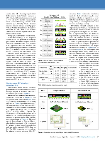
        of products. Figure 3 provides examples of
        SiP structure designs from single-sided SiP
        to double-sided SiP that enable the reduction
        in package size from 5.00 x 5.40mm
        (27mm ) to 3.60 x 3.65mm (13mm ). The
              2
                                   2
        high degree of integration along with
        achieving the required performance are
        achieved by using a double-sided stacking
        process as shown in Figure 4. The total
        area is then reduced by 50%, and better
        electrical performance (>40%) is achieved
        by using a vertical signal transmission
        path and adding a ground (GND) plane on
        L2. The RLC extraction can, therefore,
        be reduced by using a double-sided SiP
                                           Figure 4: Comparison of single-sided SiP and double-sided SiP structures.

                                                                                                             27
                                                         Chip Scale Review   September  •  October  •  2022   [ChipScaleReview.com]  27

