Page 24 - Chip Scale Review Sep Oct_2022-digital
P. 24
size of a reticle. Flip-chip bonding of extra
                                                                              large compound die on a substrate will
                                                                              become increasingly difficult as the size of
                                                                              compound die increases. A compound die
                                                                              consists of different-sized and thickness
                                                                              silicon dies and an EMC. The CTE values
                                                                              of silicon and EMC materials have a
                                                                              considerably wide range, therefore, die
                                                                              warpage will be compounded due to the
                                                                              differing degrees of expansion of the silicon
                                                                              and EMC materials.
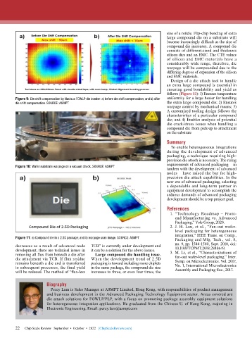
                                                                                Design of a die attach tool to handle
                                                                              an extra large compound is essential in
                                                                              ensuring good bondability and yield as
                                                                              follows (Figure 11): 1) Ensures temperature
        Figure 9: Die shift compensation by Nucleus FOWLP die bonder: a) before die shift compensation; and b) after   uniformity for a large heater for handling
        die shift compensation. SOURCE: ASMPT                                 the extra large compound die; 2) Ensures
                                                                              warpage control by mechanical means; 3)
                                                                              A customized tooling design follows the
                                                                              characteristics of a particular compound
                                                                              die; and 4) Enables analysis of potential
                                                                              die crack/stress issues when handling a
                                                                              compound die from pick-up to attachment
                                                                              on the substrate
                                                                              Summary
                                                                                To enable heterogeneous integrations
                                                                              during the development of advanced
                                                                              packaging, a technique requiring high-
                                                                              precision die attach is necessary. The rising
                                                                              requirements of advanced packaging – in
        Figure 10: Wafer substrate warpage on a vacuum chuck. SOURCE: ASMPT
                                                                              tandem with the development of advanced
                                                                              nodes – have raised the bar for high-
                                                                              precision die attach capabilities. In the
                                                                              new era of advanced packaging, selecting
                                                                              a dependable and long-term partner in
                                                                              equipment development to accomplish the
                                                                              arduous demands of advanced packaging
                                                                              development should be a top project goal.

                                                                              References
                                                                                1.  “Technology Roadmap – Front-
                                                                                  end Manufacturing vs. Advanced
                                                                                  Packaging,” Yole Group, 2020.
                                                                                2.  J. H. Lau, et al., “Fan-out wafer-
                                                                                  level packaging for heterogeneous
                                                                                  integration,” IEEE Trans. on Comp.,
        Figure 11: a) Compound die in a 2.5D package; and b) warpage scan image. SOURCE: ASMPT  Packaging and Mfg. Tech., vol. 8,
        decreases as a result of advanced node   TCB” is currently under development and   no. 9, pp. 1544-1560, Sept. 2018, doi:
                                                                                  10.1109/TCPMT.2018.2848649.
        development, there are technical issues in   it can be a solution for the above issues.  3.  M. Li, et al., “Characterizations of
        removing all flux from beneath a die after   Large compound die handling issue.   fan-out wafer-level packaging,” Inter.
        die attachment via TCB. If flux residue   When the development trend of 2.5D   Symp. on Microelectronics. Vol. 2017,
        remains beneath a die and is transferred   packaging is toward including more chiplets   No. 1, International Microelectronics
        to subsequent processes, the final yield   in the same package, the compound die size   Assembly and Packaging Soc., 2017.
        will be reduced. The method of “flux-less   increases to three, or even four times, the


                       Biography
                         Percy Lam is Sales Manager at ASMPT Limited, Hong Kong, with responsibilities of product management
                       and business development in the Advanced Packaging Technology Equipment sector. Areas covered are
                       die attach solutions for FOWLP/PLP, with a focus on promoting package assembly equipment solutions
                       for heterogeneous integration applications. He graduated from the Chinese U. of Hong Kong, majoring in
                       Electronic Engineering. Email: percy.lam@asmpt.com


        22   Chip Scale Review   September  •  October  •  2022   [ChipScaleReview.com]
        22

