Page 27 - Chip Scale Review Sep Oct_2022-digital
P. 27
Introduction                       next-generation products a reality. SiP   respect to assembly methodology to reduce
          T h e m o b i l e p ho n e a n d t a bl e t   technology realizes the characteristics of   the size and space during the product
        computer markets have matured. The   light, thin, short, multifunctional, and low   layout arrangement stage (see Figure 2). A
        next fast-growing markets will be IoT   power consumption of the entire range of   standard SiP package structure (Structure
        and wearable devices. These products   electronic products. The rise of lightweight   1) is shown in Figure 2. Its advantage is
        require a small size, a thin profile, good   products such as mobile devices and   that it uses the mature SMT process, but
        electrical properties and multi-functional   wearable devices make SiP an increasingly   the tradeoff is the design layout limitation
        requirements. From the perspective of   important packaging solution.  due to the side by side placement. Other key
        packaging development, and keeping   The current market share of smart   concerns are the small form factor as well as
        in mind the need for high-volume   watches indicates that the future of this   the thin thickness requirement that is limited
        manufacturing of electronic products,   market segment is still promising and   on a single-sided SiP. A double-sided SiP
        the processing speed, and the required   also contributes to the trend toward SiP   with one side molding (Structure 2) can
        electrical characteristics, system on a chip   packaging. An advanced SiP package   provide a smaller package (PKG) size, but
        (SoC) has been established as the key   can reduce module size and enhance the   thermal performance is the major challenge.
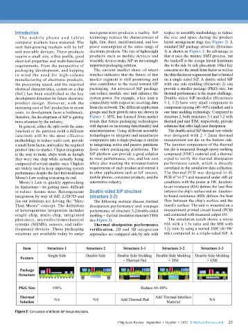
        development direction for future electronic   system power. For example, a key item is   Double-sided SiP modules (Structures
        product design. However, with the   connectivity with respect to receiving data   3-1, 3-2) have very small component to
        increasing cost of SoC production in recent   from the network. The different application   component spacing (40~60% smaller) and a
        years, its development faces a bottleneck,   groups and their growth rates are shown in   one time molding technology. Compared to
        therefore, the development of SiP is getting   Figure 1. SPIL has learned from market   structure 2, both structures 3-1 and 3-2 with
        more attention by the industry.    trends that future packaging technologies   thermal pad and TIM, respectively, provide
          In general, either die split (with the same   will depend on increasing functionality and   solutions that offer high heat dissipation.
        function) or die partition (with a different   miniaturization. Using different assembly   The double-sided SiP thermal test vehicle
        function) will be the most effective   technologies to integrate and miniaturize   was designed with 2 × 2mm thermal
        methodology to reduce wafer cost, provide   components into a single package is similar   measurement test die on the bottom side.
        a small form factor, and realize the required   to integrating active and passive partitions   The junction temperature of the thermal
        product time-to-market. Chiplet integration   from other packaging platforms. The   test die is measured through epoxy molding
        is the way to make chips work as though   SiP platform can provide a good solution   compound (EMC) material and a thermal
        they were one chip while actually being   to meet performance, size, and low cost   e-pad to verify the thermal dissipation
        composed of several smaller ones. Chiplets   while also meeting the miniaturization   performance result, which is directly
        are widely used to keep improving system   requirements of each product and extend it   correlated to the simulation data collection.
        performance despite the fact that traditional   to other applications such as IoT sensors,   The thermal PCB was designed in 4L
        Moore’s Law scaling is nearing its end.  mobile phones, consumer products, and the   PCB (4”x4.5”) and measured under still air
          Moore’s Law is quickly approaching   automotive industry.           conditions with the power at 1W. Junction-
        its limitations—its getting more difficult                            to-air resistance (θJA) defines the heat flow
        to reduce  feature sizes. Heterogeneous   Double-sided SiP structure   between the chip’s surface and air. Junction-
        integration by way of SiP, 2.5D/3D and   (structure 3-2)              to-board resistance (θJB) defines the heat
        fan-out solutions are driving the “More   The following sections discuss thermal   flow between the chip’s surface and the
        Than Moore” concept. The definition   dissipation performance and warpage   board’s surface. The unit is mounted on a
        of heterogeneous integration includes   performance of structure 3-2/double-sided   measurement printed circuit board (PCB)
        single-chip,  multi-chip,  integrated   molding + thermal insulation material (TIM)   and connected with measured output I/O.
        photonics,  microelectromechanical   (see Figure 2).                    The simulation result shows a worse
        systems (MEMS), sensors, and radio-  Thermal dissipation performance   θJA with a 1.3x ratio and the θJB with
        frequency devices. These packaging   verification. 2D and 3D integration   1.2y ratio by using a normal EMC (K=1W/
        solutions are available today to make   approaches are compared side by side with   mK) compared to a single-sided SiP. A


        Figure 2: Comparison of different SiP design structures.

                                                                                                             25
                                                         Chip Scale Review   September  •  October  •  2022   [ChipScaleReview.com]  25

