Page 22 - Chip Scale Review Sep Oct_2022-digital
P. 22
chemical shrinkage of the EMC,   D ie s y st emat ic sh i f t . D u r i ng
                                               the CTE of the carrier, gravity, the   encapsulation of a die-attached substrate,
                                               debonding process, etc.        die shift may happen and can be found
                                             •  The die shift caused by the CTE   after debonding of the molded substrate
                                               mismatch between the EMC and   (Figure 8). Oftentimes, the trend of die
                                               silicon, which is also influenced by   shift can be observed to be systematic.
                                               chemical shrinkage of the EMC, the   The major contributing factor is material-
                                               type of EMC, and the thermal release   related shrinkage of the carrier, adhesive
                                               tape in use.                   and EMC. Fortunately, the issue can be
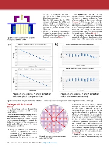
                                             •  The amount of die shift compensation   predicted and compensation provided
                                               that can be accomplished by using   during die pick-and-place (Figure 9).
                                               intelligent offset introduced during the   Wafer substrate warpage handling
                                               die attach process (see Figure 7).  capability. Substrate handling is often
        Figure 6: Needle-less ejector system for handling                     complicated by substrate warpage.
        thin-die pick up. SOURCE: ASMPT


        Figure 7: Die systematic shift position offset data in the X and Y directions: a) without pitch compensation; and b) with pitch compensation. SOURCE: [3]

        Challenges with the die attach                                        Oftentimes substrate warpage can be
        process                                                               as large as up to five millimeters. This
          The following sections discuss the                                  serious  issue is  basically  related  to
        challenges associated with the die                                    the complicated structure for the AP
        attach process.                                                       application where it is no longer a bare
          Die shift in fan-out packaging (wafer-                              silicon or glass carrier. For example, the
        and panel-level fan-out). There are still                             substrate can be fabricated with multilayer
        many different aspects of process, material                           RDLs with asymmetric metal density.
        and equipment development needed for                                  Or, the substrate can have unevenly
        further improvement of fan-out packaging                              distributed embedded components. Such
        quality and yield improvement. The major                              structural differences will lead to warpage
        challenges are as follows:                                            either at room temperature or at elevated
                                                                              temperatures. Machine design, therefore,
          •  Warpage caused by a mismatch                                     requires appropriate attention to such
            between the coefficient of thermal                                mechanical and process considerations
            expansion (CTE) for the epoxy mold                                (Figure 10).
            compound (EMC) and silicon.                                         Flux-cleaning issue. When the
          •  Impact on the process caused by   Figure 8: Directions of die shift from the wafer’s   die size increases and the bump pitch
                                           center. SOURCE: ASMPT

        20
        20   Chip Scale Review   September  •  October  •  2022   [ChipScaleReview.com]

