Page 9 - Chip Scale Review_March April_2022-digital
P. 9
beg u n  to be  applied  for package
        substrates using build-up polymer
        dielectrics, large-area photolithography
        and semi-additive processes, leading to
        about 10µm wiring widths, currently.
        Wafer–based BEOL packaging has
        always been below 1µm using dry
        processes for inorganic dielectrics
        and the dual-damascene processes.
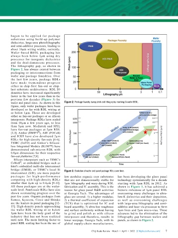
        The lithography gap, as shown in
        Figure 2, has always existed between
        packaging or interconnections from
        wafer and package foundries. Over
        the last few years, package RDLs
        have ma de t remendou s prog ress
        either in chip-first fan-out or chip-
        last substrate architectures. RDL IO
        densities have increased significantly
        faster in the last few years than in the
        previous few decades (Figure 3) for
        wafer and panel sizes. As shown in this   Figure 2: Package foundry bump pitch and lithography reaching Si wafer BEOL.
        figure, only wafer packages have been
        developed so far with RDL wiring at
        or below 1µm. These are developed
        either as fan-out packages or as silicon
        interposers. Package RDLs have scaled
        from 10µm a few years ago, to less
        than 5µm now. Mediatek and SPIL
        have fan-out packages at 5µm RDL
                          ®
        [2,3]. Amkor (SWIFT ), ASE (FOCoS)
        and JCET  have also developed  2µm
        RDLs for high-density fan-outs [4-6].
        TSMC (InFO) and Amkor’s Silicon-
        less Integrated Module (SLIM™) have
        demonstrated sub-micron RDL with
        0.8µm dimensions for their respective
        fan-out platforms [7,8].
          Silicon interposers such as TSMC’s
              ®
        CoWoS , or embedded bridges such as
        Intel’s embedded multi-die interconnect
        bridge (EMIB), or TSMC’s local Si   Figure 3: Evolution of wafer and panel package RDLs over time.
        interconnect (LSI), are more popular
        p a ck a ge s fo r h ig h - p e r fo r m a n c e   low modulus organic core substrates   has been developing the glass panel
        computing with high-density RDLs   that are not dimensionally stable for   technology systematically for a decade
        smaller than 2µm up to 0.4µm [9-11].   1µm lithography and warp during RDL   starting with 5µm RDL in 2012. As
        All these packages are at the wafer-  fabrication and IC assembly. This is the   shown in Figure 3, it has achieved a
        scale level. Panel-scale RDLs have also   reason for glass panel R&D activities   historic milestone of 1µm panel RDL
        shown outstanding progress over the   at Georgia Tech. The advantages of   overcoming many challenges in ultra-
        past few years. Organic packages from   glass are several: 1) a higher modulus;   low-K dielectrics and their deposition,
        Semco, Kyocera, Cisco and Shinko   2) a thermal coefficient of expansion   as well as overcoming challenges
        are the leaders in panel packaging [12-  (TCE) that is optimized for IC and   with large-area lithography and semi-
        15]. High-density panels approaching   board assembly; 3) ultra-low roughness   additive and laser via processes to form
        the wafer RDL wiring at or below   and surface uniformity without having   1µm lines and 2µm micro-vias. These
        1µm have been the holy grail of the   to grind and polish as with silicon   advances led to the elimination of the
        industry that has not been realized   interposers and therefore, results in   lithography gap between wafers and
        until now. The main limiting factor to   lower warpage. Georgia Tech, with its   panels, as shown in Figure 2.
        panel RDL scaling has been the use of   global supply-chain manufacturers,

                                                             Chip Scale Review   March  •  April  •  2022   [ChipScaleReview.com]  7 7

