Page 11 - Chip Scale Review_March April_2022-digital
P. 11
Tech to further scale RDL dimensions
                                                                              below 1µm using advances in SAP on
                                                                              glass panels. Simultaneously, glass panel
                                                                              packaging is also gaining momentum in
                                                                              the industry with Asian and American
                                                                              companies gearing up to manufacture
                                                                              these latest panels, starting in 2022.
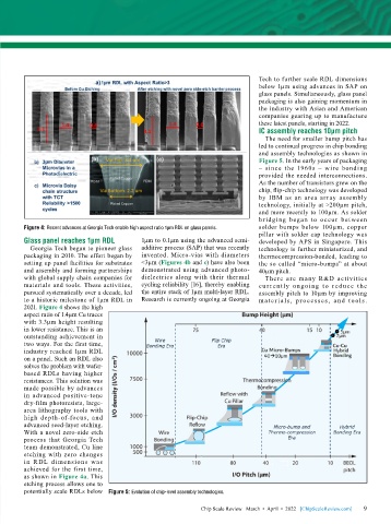
                                                                              IC assembly reaches 10µm pitch
                                                                                The need for smaller bump pitch has
                                                                              led to continual progress in chip bonding
                                                                              and assembly technologies as shown in
                                                                              Figure 5. In the early years of packaging
                                                                              – since the 1960s – wire bonding
                                                                              provided the needed interconnections.
                                                                              As the number of transistors grew on the
                                                                              chip, flip-chip technology was developed
                                                                              by  IBM  as  an  area  array  assembly
                                                                              technology, initially at >200µm pitch,
                                                                              and more recently to 100µm. As solder
                                                                              bridging  began  to  occur  between
        Figure 4: Recent advances at Georgia Tech enable high aspect ratio 1µm RDL on glass panels.  solder bumps below 100µm, copper
                                                                              pillar with solder cap technology was
        Glass panel reaches 1µm RDL        1µm to 0.1µm using the advanced semi-  developed by APS in Singapore. This
          Georgia Tech began to pioneer glass   additive process (SAP) that was recently   technology is further miniaturized, and
        packaging in 2010. The effort began by   invented. Micro-vias with diameters   thermocompression-bonded, leading to
        setting up panel facilities for substrates   <3µm (Figures 4b and c) have also been   the so called “micro-bumps” at about
        and assembly and forming partnerships   demonstrated using advanced photo-  40µm pitch.
        with global supply chain companies for   dielectrics along with their thermal   There are many R&D activities
        materials and tools. These activities,   cycling reliability [16], thereby enabling   cu r rently ongoi ng to reduce t he
        pursued systematically over a decade, led   the entire stack of 1µm multi-layer RDL.   assembly pitch to 10µm by improving
        to a historic milestone of 1µm RDL in   Research is currently ongoing at Georgia   mater ials, processes, a nd tools.
        2021. Figure 4 shows the high
        aspect ratio of 1.4µm Cu traces
        with 3.3µm height resulting
        in lower resistance. This is an
        outstanding achievement in
        two ways. For the first time,
        industry reached 1µm RDL
        on a panel. Such an RDL also
        solves the problem with wafer-
        based RDLs having higher
        resistances. This solution was
        made possible by advances
        in advanced positive-tone
        dry-film photoresists, large-
        area lithography tools with
        high depth-of-focus, and
        advanced seed-layer etching.
        With a novel zero-side etch
        process that Georgia Tech
        team demonstrated, Cu line
        etching with zero changes
        in R DL dimensions was
        achieved for the first time,
        as shown in Figure 4a. This
        etching process allows one to
        potentially scale RDLs below  Figure 5: Evolution of chip-level assembly technologies.

                                                             Chip Scale Review   March  •  April  •  2022   [ChipScaleReview.com]  9 9

