Page 8 - Chip Scale Review_March April_2022-digital
P. 8
TECHNOLOGY TRENDS


                           A new and historic packaging era


                           By Rao Tummala, Madhavan Swaminathan, Pratik Nimbalkar  [Georgia Institute of Technology]


        A         n e w , h i s t o r i c , a n d


                  transformative packaging
                  era has beg u n star ting
                  with high-perfor mance
        c om p u t i n g  e l e c t r o n i c s.  T h i s
        transformation is due to many reasons
        that include the transistor speed slowing
        down  from node  to  node,  thereby
        contributing to slowdown in computing
        performance, and the increase in chip
        size along with an increase in the number
        of transistors to more than 50 billion
        with the concurrent increase in their
        cost. The slowdown in transistor speed
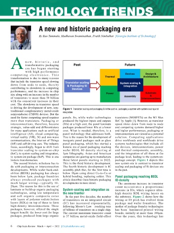
        is driving the development of new, non-  Figure 1: Transistor scaling and packaging Si in the past vs. packaging a system with system scaling and
        traditional complementary metal-oxide   integration.
        semiconductor (CMOS) devices. But the
        need for faster computing speed requires   panels. So, while wafer technologies   transistors (MOSFETs) on the M1 Max
        more than transistors. Packaging or   produced the highest inputs and outputs   SoC by Apple [1]. However, as transistor
        interconnections, therefore, became   (IOs) at a high cost, the panel laminate   speed slows down from node to node
        strategic, value-add and differentiators   packages produced lower IOs at a lower   and computing systems demand higher
        for many applications such as artificial   cost. What is needed, therefore, is a   and higher performances, packaging or
        intelligence (AI), cloud computing,   panel technology that addresses both.   interconnections are viewed as a potential
        virtual reality (VR), 5G and mm-wave   This is the reason for the development of   solution. Computing applications
        communications, the Internet of Things   inorganic panel packages such as glass   drive workloads and workloads drive
        (IoT) and self-driving cars. The industry   panel packaging, which has started a   systems technologies that include all
        focus, accordingly, began to shift from   historic era of panel packaging reaching   the devices, interconnections, power
        transistor scaling to system-on-chip   wafer BEOL IO  density starting at   and  thermal components, assembly,
        (SoC), to system scaling and integration,   1µm lithography. Asian and American   and the integration of all these at the
        to system-on-package (SoP). This is one   companies are gearing up to manufacture   package level, leading to the system-on-
        historic transformation.           these latest panels starting in 2022.   package concept. Figure 1 depicts this
          The second historic milestone has to   This is the third historic development.   new system era in contrast to transistor
        do with packaging or interconnection   The fourth historic development is IC   scaling and packaging of Si devices era
        developments. While wafer back-end-  assembly pitch that, for the first time is   in the past.
        of-line (BEOL) packaging has always   below 10µm using direct Cu-to-Cu or
        been below 1µm, package foundries   hybrid bonding, replacing solder. This   Panel packaging reaching BEOL
        always pro duce d pa ck age s w it h   article describes these historic packaging   IO-density
        much larger wiring—typically 10-   developments in more detail.         The enormous increase in transistor
        20µm. The reason for this is the use of                               count necessitates  a  proportional
        laminate or build-up organic packaging   System-scaling and integration as   increase in IOs, which requires ultra-
        technologies, using low temperature   the new frontier                high density RDL wiring layers on
        and soft organic composite cores     In the past five decades, the number   the substrate. Figure 2 shows how the
        with layers of polymer redistribution   of transistors on an integrated circuit   wiring or IO pitch has evolved from
        layers (RDLs) on top of these to form   (IC)  has  increased  exponentially,   package and wafer foundries. The
        high-density interconnections. These   following Moore’s Law—reaching tens   mother of package foundry technologies
        packages, however, offered the single   of billions of transistors on a single chip.   has been  laminated printed wiring
        largest benefit: the lower cost for large   The current maximum transistor count   boards, initially at more than 100µm.
        packages, produced from large organic   is 57 billion metal-oxide field-effect   Over the years, this technology has


        6 6  Chip Scale Review   March  •  April  •  2022   [ChipScaleReview.com]

