Page 47 - Chip Scale Review_January February_2022-digital
P. 47
The mathematical operations to be   NN. For such an architecture to work, the   stored along the word lines can be multiplied
        performed in a DNN include matrix-vector   HBM and logic must be connected using   with the matrix elements programmed
        multiplication (WX), addition (WX+b), a   short wires through an interposer as shown   into the conductance cells through current
        pointwise operation as in activation using   in the figure to reduce off-chip memory   summing, with the output available through
        ReLU, sigmoid and others and fully-  latency. For an HBM configuration that has   the bit lines. For a large matrix that does not
        connected layers using batch matrix   four memory stacks, each having 8 channels   fit into the array of the crossbar structure
        multiplication. A NN may also include   that contain 128-bit data interface [6], it   multiple arrays can be used where partial
        convolutional layers as in CNN, which   has been shown that the achievable total   sums can be added to obtain the output [5].
        involves matrix-vector multiplication   bandwidth aggregates to 1.63TB/s using a   Several possibilities arise in the
        using a sparse, or Toeplitz matrix [5]. In a   silicon interposer [7].  implementation of the PIM architecture
        NN, around 80-90% of the computations   A method for reducing off-chip latency is   with two of them described in [7] namely:
        are related to matrix multiplications and   by using the hybrid memory cube (HMC)   1) A single PIM engine coupled with a
        convolution while the remaining 10-20% are   based on the Neurocube architecture   DRAM module used to store the DNN
        used in the computation of vector functions   that integrates logic within a 3D-stacked   parameters and establishes connections
        such as ReLU, sigmoid and others. Rather   DRAM memory. Here, each Neurocube   through an interposer similar to Figure
        than using a general-purpose CPU for such   accelerator contains one HMC containing   2a with the logic replaced by PIM; and
        computations, accelerator chips can be used   16 vaults, where each vault consists of a PE   2) Multiple PIM accelerators where all
        with smaller dies from advanced process   that performs multiplication-accumulation   the DNN parameters are stored within
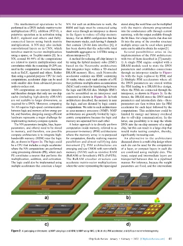
        nodes to reduce cost.              (MAC) and a router for transferring between   the PIM leading to a DRAM-free design,
          NN computations are memory intensive   the logic and DRAM dies. Multiple HMCs   where the PIMs are connected through the
        and therefore designs that only use on-chip   can be assembled on an interposer and   interposer, as shown in Figure 2c. In the
        cache (including high-density eDRAM)   connected as shown in Figure 2b. In both   former, the DRAM stores the DNN model
        are not scalable to larger dimensions, as   architectures described, the memory is near   parameters and intermediate data—these
        required for a DNN. Moreover, computing   the logic, and are dictated by logic centric   parameters are then written into the PIM
        for AI requires high-speed communication   computations. We refer to such architectures   accelerator for each layer followed by the
        between logic and memory at low energy per   as near-memory processor (NMP). NMP   computations. This architecture could be
        bit, and therefore, designing energy-efficient   architectures are generally limited by logic-  limited by energy and latency overhead
        hardware represents a major challenge for   centric computations because the logic and   due to off-chip communication. In the
        implementing memory-compute systems.  memory are separated from each other.  latter, one possibility is to map the whole
          The NN parameters (weights, bias, hyper-  A better approach is to directly perform   DNN into the on-chip memory of a single
        parameters, and others) need to be stored   computation inside memory, referred to as   chip, but this can result in a large chip that
        in memory, and therefore, one possible   processor-in-memory (PIM) architectures   would make testing complex, thereby,
        compute architecture is to integrate high-  where the memory array is re-purposed   significantly increasing cost.
        bandwidth memory (HBM) near the logic   for computation, thereby realizing massive   An alternative to the architecture
        die, as shown in Figure 2a. The logic could   parallelism and almost nullifying data   discussed above is a multi-chip design where
        be a CPU that includes a single accelerator   movement [7]. PIM architectures are   each die can be used for the computation
        where the NN computations are performed   emerging and use CMOS with non-volatile   of a layer, or compact layers in each die
        using processing elements (PE), where each   memory (NVM) such as resistive RAM   are combined using multiple dies. The
        PE constitutes a neuron that performs the   (ReRAM) or ferroelectric FETs (FeFETs).   input, output and intermediate layers are
        multiplication, addition, and activation.   The ReRAM crossbar structure can   transported between dies in a pipelined
        The logic could also be implemented using   accelerate matrix-vector multiplications   manner. For inference, because the weight
        multiple accelerators that constitute a larger   where the vector representing the input signal   parameters are fixed, and the intermediate


        Figure 2: AI packaging architectures: a) NMP using logic and HBM; b) NMP using HMC; c) Multi-chip PIM accelerator; and d) Future extreme heterogeneity.

                                                                                                             45
                                                          Chip Scale Review   January  •  February  •  2022   [ChipScaleReview.com]  45

