Page 43 - Chip Scale Review_January February_2022-digital
P. 43
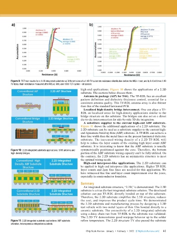
Figure 9: TCT test results for a 2.2D integrated substrate: a) Different sizes of a 2.2D TV substrate resistance distribution before the MSL 4 test; and b) A 20x20mm 2.2D
        TV daisy chain resistance measured after MSL4, 500, and 1000 TCT cycles—all passed.
                                                      high-end applications. Figure 10 shows the applications of a 2.2D
                                                      substrate. The sections below discuss them.
                                                        Antenna in package (AiP) for 5/6G. The TF-RDL has an excellent
                                                      pattern definition and dielectric thickness control, essential for a
                                                      consistent antenna quality. This TF-RDL antenna array is also thinner
                                                      than that of the standard laminated PCB.
                                                        Localized high-density bridge interconnect. One can place a TF-
                                                      RDL on localized areas for high-density applications similar to the
                                                      bridge structure on the substrate. The bridges can also act as a direct
                                                      die-to-die interconnection for side-by-side 3D die integration.
                                                        A substitute supplier to the current high-end ABF substrate.
                                                      Figure 11 shows the additional applications of a 2.2D substrate. The
                                                      2.2D substrate can be used as a substitute supplier to the current high-
                                                      end Ajinomoto build-up film (ABF) substrate. A TF-RDL can achieve a
                                                      finer line width than the metal lines on the present laminated dielectric
                                                      substrate. The increased wiring density of a 2.2D TF-RDL will
                                                      help to reduce the layer counts of the existing high layer count ABF
                                                      substrate. It is interesting to know that the ABF substrate is usually
        Figure 10: 2.2D integrated substrate applications: 5/6G antenna and   symmetrically positioned against the core. Therefore, the bottom
        high-density bridges.                         portion of the ABF substrate wiring capacity can’t be fully utilized. On
                                                      the contrary, the 2.2D substrate has an asymmetric structure to meet
                                                      the optimal wiring needs.
                                                        High-end interposer-like applications. The 2.2D substrate can
                                                      be applied to high-end interposer-like applications. Higher TF-RDL
                                                      layer counts and 2µm fine lines are needed for this application. We
                                                      have witnessed fine line and layer count improvement over the years,
                                                      especially in semiconductor foundries.

                                                      Summary
                                                        An integrated substrate structure, “2.2D,” is demonstrated. The 2.2D
                                                      substrate is a true die-last integrated substrate solution. The developed
                                                      solution can put TF-RDL directly bonded on top of the substrate.
                                                      Therefore, the 2.2D substrate simplifies the 2.5D structure, reduces
                                                      the cost, and improves the product cycle time. We demonstrated
                                                      the 2.2D substrate and manufacturing process by designing a 2.2D
                                                      test vehicle with two metal layers of thin film bonded directly to a
                                                      ceramic substrate. The connectivity of a 2.2D integrated substrate
                                                      using a daisy chain run from TF-RDL to the substrate was validated.
                                                      The 2.2D TV demonstrates good warpage behavior up to the solder
        Figure 11: 2.2D integrated substrate applications: ABF substrate   reflow temperature. The 2.2D structure TV also passed the substrate
        alterative, heterogeneous integration substrate.

                                                                                                             41
                                                          Chip Scale Review   January  •  February  •  2022   [ChipScaleReview.com]  41

