Page 52 - Chip Scale Review_January February_2022-digital
P. 52
shown in Figure 1. The silicon buffer is just an additional
                                                             section of the Si substrate of the PIC, extending beyond
                                                             the edge optical coupling circuit. The PIC with this buffer
                                                             section design is then embedded in the FOWLP process.
                                                             The PIC buffer section protects the optical I/Os and
                                                             will only be diced off during the singulation, or dicing
                                                             process, to expose the PIC optical I/Os. Depending on the
                                                             application requirement, the EIC can be either embedded
                                                             side by side with the PIC, or integrated on top of the
                                                             FOWLP PIC.
                                                               The extended mold area of the FOWLP is used to support
                                                             the electrical lateral and vertical routing connections
                                                             using the redistribution layer (RDL). The RDL can provide
                                                             very fine line width connections and reduce the parasitic
                                                             components with good impedance control for high-speed
                                                             connections. The PIC and EIC can be integrated laterally
                                                             with a gap of less than 500μm. In this way, it can achieve a
                                                             very short electrical length and a well-matched interconnect
                                                             to support the high-speed and high-density integration.
                                                             Through-mold vias (TMVs) can be designed on the FOWLP
        Figure 1: Schematic showing the FOWLP embedding solution of PIC with edge   and the EIC can be stacked directly on top of the PIC for 3D
        optically-coupled I/Os.                              integration. Although this can help to reduce the package
                                                             size, it increases the design and process complexity.
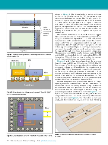
                                                               Figures 2 and  3 show the schematic of the proposed
                                                             laterally-integrated PIC and EIC using the FOWLP. The EIC
                                                             here consists of the driver for the photonics modulator and
                                                             the transimpedance amplifier (TiA) for the photodetector in
                                                             the EIC. The FOWLP is designed for the flip-chip assembly
                                                             on the substrate. Flip-chip assembly is preferred as it can
                                                             provide high-speed and high-bandwidth connection to the
                                                             switch IC or ASIC on the mainboard. In addition, the flip-
                                                             chip assembly allows the heat sink to be designed directly on
                                                             the backside of the EIC to reduce thermal effects.
                                                               For the integration design described above, the high-
                                                             speed signal lines between the PIC and EIC, and the EIC to
                                                             the external circuit, are usually designed using a differential
                                                             transmission line. The performance of the differential
                                                             transmission lines of 1.0mm length is modeled using a 3D
        Figure 2: Schematic side view of the proposed integrated PIC and EIC FOWLP   (electromagnetic) EM simulator as shown in Figure 4. The
        flip-chip attached to the substrate.                 typical dielectric constant and the loss tangent of the mold
                                                             compound are around 3.4 and 0.008, respectively. The simulated
                                                             results are shown in Figure 5. The return loss is more than
                                                             30dB, and the insertion loss ranges from less than 0.15dB up


                                                             Figure 4: Simulation model of a differentiated GSSG transmission line design
        Figure 3: Schematic bottom view of the FOWLP with PIC and EIC (TiA and driver).  on FOWLP.

        50   Chip Scale Review   January  •  February  •  2022   [ChipScaleReview.com]
        50

