Page 56 - Chip Scale Review_January February_2022-digital
P. 56
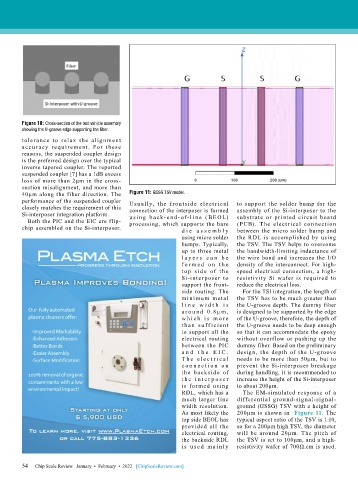
Figure 10: Cross-section of the test vehicle assembly
        showing the U-groove edge supporting the fiber.
        tolerance to relax the alig n ment
        accu racy requirement.  For  these
        reasons, the suspended coupler design
        is the preferred design over the typical
        inverse tapered coupler. The reported
        suspended coupler [7] has a 1dB excess
        loss of more than 2μm in the cross-
        section misalignment, and more than
        40μm along the fiber direction. The   Figure 11: GSSG TSV model.
        performance of the suspended coupler   Usually, the f rontside elect r ical   to support the solder bump for the
        closely matches the requirement of this   connection of the interposer is formed   assembly of the Si-interposer to the
        Si-interposer integration platform.  u si n g b a ck- e n d - of-l i n e ( BE OL)   substrate or printed circuit board
          Both the PIC and the EIC are flip-  processing, which supports the bare   (PCB). The electrical connection
        chip assembled on the Si-interposer.                d i e  a s s e m b l y   between the micro solder bump and
                                                            using micro solder   the RDL is accomplished by using
                                                            bumps. Typically,   the TSV. The TSV helps to overcome
                                                            up to three metal   the bandwidth-limiting inductance of
                                                            l a y e r s c a n b e   the wire bond and increases the I/O
                                                            f o r m e d o n  t h e   density of the interconnect. For high-
                                                            t o p sid e of t he   speed electrical connection, a high-
                                                            Si-inter poser to   resistivity Si wafer is required to
                                                            support the front-  reduce the electrical loss.
                                                            side routing. The   For the TSI integration, the length of
                                                            minimum metal     the TSV has to be much greater than
                                                            l i n e w i d t h i s   the U-groove depth. The dummy fiber
                                                            a r ou n d  0 . 8 μ m ,   is designed to be supported by the edge
                                                            w h i c h i s m o r e   of the U-groove, therefore, the depth of
                                                            t h an s u f f icie nt   the U-groove needs to be deep enough
                                                            to support all the   so that it can accommodate the epoxy
                                                            electrical routing   without overflow or pushing up the
                                                            between the PIC   dummy fiber. Based on the preliminary
                                                            a n d t h e EI C .   design, the depth of the U-groove
                                                            T h e  e le c t r i c a l   needs to be more than 50μm, but to
                                                            c on n e c t i on  on   prevent the Si-interposer breakage
                                                            the backside of   during handling, it is recommended to
                                                            t h e   i n t e r p o s e r   increase the height of the Si-interposer
                                                            is for med using   to about 200μm.
                                                            RDL, which has a    The EM-simulated response of a
                                                            much larger line   differential ground-signal-signal-
                                                            width resolution.   ground (GSSG) TSV with a height of
                                                            As most likely the   200μm is shown in  Figure 11. The
                                                            top side BEOL has   typical aspect ratio of the TSV is 1:10,
                                                            provided all the   so for a 200μm high TSV, the diameter
                                                            electrical routing,   will  be  around  20μm.  The  pitch  of
                                                            the backside RDL   the TSV is set to 100μm, and a high-
                                                            i s u s e d m a i n ly   resistivity wafer of 700Ω.cm is used.


        54   Chip Scale Review   January  •  February  •  2022   [ChipScaleReview.com]
        54

