Page 53 - Chip Scale Review_January February_2022-digital
P. 53

if necessary. It is used to prevent the
                                                                              underfill in the subsequent step from
                                                                              f lowing  to  the  optical  I/O  area,  or
                                                                              protected area. The singulation process
                                                                              is designed so that the PIC buffer area
                                                                              together with its surrounding mold are
                                                                              diced off at Step 7. The FOWLP of the
                                                                              EIC and PIC with optical edge coupling
                                                                              is then formed. The integrated photonics
                                                                              FOWLP module can then be flip-chip
                                                                              assembled to the main optical board or
                                                                              substrate for the main integration. The
                                                                              process described above is compatible
                                                                              with the FOWLP process. IME is
                                                                              currently developing the complete
                                                                              process and evaluating the optical
                                                                              coupling performance.
                                                                                Figure 7a shows the PIC test vehicle
                                                                              after the FOWLP molding process
                                                                              before the dicing is done. The buffer
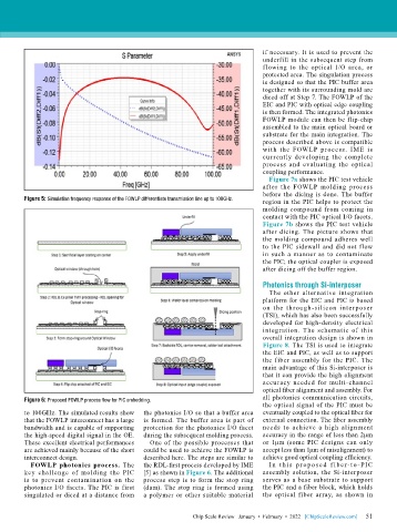
        Figure 5: Simulation frequency response of the FOWLP differentiate transmission line up to 100GHz.  region in the PIC helps to protect the
                                                                              molding compound from coming in
                                                                              contact with the PIC optical I/O facets.
                                                                              Figure 7b shows the PIC test vehicle
                                                                              after dicing. The picture shows that
                                                                              the molding compound adheres well
                                                                              to the PIC sidewall and did not flow
                                                                              in such a manner as to contaminate
                                                                              the PIC; the optical coupler is exposed
                                                                              after dicing off the buffer region.

                                                                              Photonics through Si-interposer
                                                                                The other alternative integration
                                                                              platform for the EIC and PIC is based
                                                                              on  the  through-silicon inter poser
                                                                              (TSI), which has also been successfully
                                                                              developed for high-density electrical
                                                                              integration. The schematic of this
                                                                              overall integration design is shown in
                                                                              Figure 8. The TSI is used to integrate
                                                                              the EIC and PIC, as well as to support
                                                                              the fiber assembly for the PIC. The
                                                                              main advantage of this Si-interposer is
                                                                              that it can provide the high alignment
                                                                              accuracy needed for multi-channel
                                                                              optical fiber alignment and assembly. For
                                                                              all photonics communication circuits,
        Figure 6: Proposed FOWLP process flow for PIC embedding.
                                                                              the optical signal of the PIC must be
        to 100GHz. The simulated results show   the photonics I/O so that a buffer area   eventually coupled to the optical fiber for
        that the FOWLP interconnect has a large   is formed. The buffer area is part of   external connection. The fiber assembly
        bandwidth and is capable of supporting   protection for the photonics I/O facet   needs to achieve a high alignment
        the high-speed digital signal in the OE.   during the subsequent molding process.  accuracy in the range of less than 2μm
        These excellent electrical performances   One of the possible processes that   or  1μm  (some  PIC  designs  can  only
        are achieved mainly because of the short   could be used to achieve the FOWLP is   accept less than 1μm of misalignment) to
        interconnect design.               described here. The steps are similar to   achieve good optical coupling efficiency.
          FOWLP  photonics  process.  The   the RDL-first process developed by IME   I n t h is p rop o se d f ib e r-t o -PIC
        key challenge of molding the PIC   [5] as shown in Figure 6. The additional   assembly solution, the Si-interposer
        is to prevent contamination on the   process step is to form the stop ring   serves as a base substrate to support
        photonics I/O facets. The PIC is first   (dam). The stop ring is formed using   the PIC and a fiber block, which holds
        singulated or diced at a distance from   a polymer or other suitable material   the optical fiber array, as shown in


                                                                                                             51
                                                          Chip Scale Review   January  •  February  •  2022   [ChipScaleReview.com]  51
   48   49   50   51   52   53   54   55   56   57   58