Page 49 - Chip Scale Review_January February_2022-digital
P. 49
the figure, R on  is the driver resistance while C Tx  and C Rx  are the driver
        and receiver capacitances, respectively. The interconnections are
        designed with minimum dimensions, where five coupled lines carry
        the signals in parallel. The RC parameters of the line are extracted
        using an electromagnetic (EM) simulator [10] and the eye-diagram
        at the far end of the center line is computed using the wirelengths
        derived from Eq. 3. The maximum data rate per IO that can be
                                            -12
        supported based on a bit error rate (BER) of 10  is then computed
        by increasing the signal frequency until the EH mask  and EW shown in
        Figure 4b reach 0.1V in  (along the vertical voltage axis) and 0.1UI (UI
        = unit interval along the horizontal time axis), respectively. Because
        the linewidths and spacing are small, the interconnect response
        is RC dominated as can be seen from the eye-diagram. (In part 2
        of this article [Tables 2 and 3], we will show that the difference in
        data rate/IO between the various 2D and 3D approaches is due to
        dielectric permittivity (scales C), L/S (scales R & C), driver/receiver
        parameters and linelength.)
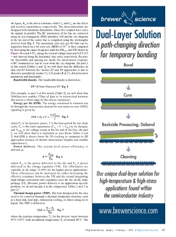
          Bandwidth density. The bandwidth density is derived as:

                     BW=IO/mm×Datarate/IO  Eq. 4

        (For example, in part 2 of this article [Table 2], we will show that
        500Gbps/mm enables 5Tbps of data to be transmitted between
        dies across a 10mm edge for the silicon interposer.)
          Energy per bit (EPB). The energy consumed to transmit one
        bit through the interconnect channel for non-return to zero (NRZ)
        signaling is given by:

                                           Eq. 5

        where P D  is the dynamic power, T is the time period for one clock
        cycle, C T  is the total capacitance (C Tx  + C + C Rx ) to be charged,
        and V swing  is the voltage swing at the far end of the line. (In part
        2, we will show that it is important to note [from Tables 2 and
        3] that EPB is always lower for 3D stacking as compared to 2D
        approaches because of shorter interconnect lengths and smaller
        capacitances.)
          Power delivery. The system level power efficiency is
        defined as:

                                       Eq. 6
        where P out  is the power delivered to the die and P in  is power
        delivered to the voltage regulator (VR). The efficiencies are
        typically in the range 75-80% for the higher power applications.
        These efficiencies can be increased by either decreasing the
        effective resistance between the VR and die or/and integrating
        high-voltage conversion ratio regulators near the die on the same
        package [11]. (Because power delivery is an application-specific
        problem, we do not include it in the comparison Tables 2 and 3 in
        part 2.)
          Thermal design power (TDP). The heat dissipated by the dies
        need to be removed through a thermal dissipation structure such
        as a heat sink, heat pipe, immersion cooling, or others using air or
        liquid. The TDP is defined as:

                                         Eq. 7
        where the junction temperature, T j , for the devices varies between
        85°C-130°C with an ambient temperature T a  of around 40°C. The


                                                                                                             47
                                                          Chip Scale Review   January  •  February  •  2022   [ChipScaleReview.com]  47

