Page 48 - Chip Scale Review_January February_2022-digital
P. 48
data size is smaller than the weight
        parameters, the data communication latency
        and energy can be reduced. In [7], it has been
        shown that for AlexNet, a CNN implemented
        using a FeFET-based PIM accelerator, the
        multi-chip design leads to lower energy
        efficiency and latency as compared to a
        single-chip design. In addition, the multi-
        chip design provides higher throughput
        because of pipelined execution.
          In both NMP and PIM accelerator
        architectures, the DRAM, logic, and other
        dies come from different process nodes
        and are connected using 2D (interposer
        and package substrate) or 3D (stacking)
        leading to heterogeneous integration. As AI
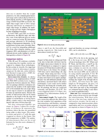
        architectures become more prevalent there   Figure 3: Interconnect density and wiring length.
        will be a need for integrating additional   where L and S are the linewidth and   equal and therefore, an average wirelength,
        dies from other domains (analog, radio   spacing, respectively. This leads to an   AWL, can be calculated as:
        frequency (RF), and photonics), as well as   interconnect density per layer:
        different process nodes leading to extreme
        heterogeneity as shown in Figure 2d.                                                              Eq. 3
                                                                  Eq. 2
                                                                              where DS is the die-to-die spacing, and
        Comparison metrics                 (In part 2 of this article we will present Table   K is the keep-out zone (KOZ). Most
          With 2D and 3D solutions available   2; the data in that table will show that the   advanced packages have DS=100μm and
        for connecting dies together, metrics are   10X higher interconnect density for silicon   K=50μm, and therefore, n and P are the
        required to compare these technologies.   (250 IO/mm/layer) as compared to organic   main parameters that affect AWL. As
        In this section we describe five important   interposer (25 IO/mm/layer) results in the use   more columns in each die are routed,
        metrics related to interconnect density,   of fewer layers in the former. For example,   AWL will increase, but compensation
        energy per bit, data rate, power delivery,   7,500 wires can be routed along a die edge   for the increased AWL can be achieved
        and thermal design power (TDP) for   of length 10mm using just three wiring   by using smaller pad pitch, P. For 3D
        comparing the various options.     layers with a silicon interposer as compared   stacking, the wirelength is the physical
          Interconnection density. As shown   to many more layers in an organic package.   length that connects dies together, which
        in Figure 2, the implementation of NMP   Because vias add additional parasitic losses   includes the length of the through-silicon
        and PIM DNN architectures requires   and latency, increased layers will reduce   via (TSV). All wires have the same
        connectivity between adjacent dies. When   performance. Layer count can be further   length in 3D integration. (In part 2 of
        dies on a package substrate or interposer are   reduced by decreasing the assembly pitch.   this article, we will present Tables 2 and
        connected, the number of die input/output   For 3D stacking, the dies are connected   3 that show that some of the wirelengths
        (I/O or IO) terminals that can escape along   vertically, and therefore, W=(1⁄P) . For   are estimated based on Eq. 3, and others
                                                                       2
        the die edge to connect to an adjacent die   a non-staggered pitch of P=10μm, this   are based on published data.)
        becomes an important metric. Because the   translates to an interconnection density of   Data rate. Dies communicate with each
        number of interconnects that can be routed   10,000 IO/mm .)          other using a driver-receiver pair through
                                                      2
        depends on the length of the die edge and   Interconnect length. The length of the   the interconnection. With short wires
        number of redistribution or wiring layers   wire connecting adjacent dies determines   that are a few mm long, simple driver
        (RDL), a better metric is the interconnect   the total resistance and capacitance of the   and receiver circuitry can be used, as
        density with units of IO/mm/layer [8].   interconnections, and therefore, represents   compared to long interconnections where
          Two  dies connected  together  are   an important design parameter to consider.   equalization and error correction schemes
        shown in Figure 3 where the circular   From Figure 3, not all wire lengths are   are required, as shown in Figure 4a [9]. In
        pads of diameter D represent the
        positions where the dies are assembled
        using solder or other means. The center-
        to-center pad pitch is P with the pads
        staggered as shown in the figure, like
        pad arrangements in HBM. The number
        of interconnects that can be wired
        between the two dies over a distance. P y
        is given by:

                             Eq. 1

                                           Figure 4: a) Driver-interconnect-receiver communication, and b) Eye diagram at the far end of the center line.

        46
        46   Chip Scale Review   January  •  February  •  2022   [ChipScaleReview.com]

