Page 52 - ChipScale_Nov-Dec_2020-digital
P. 52
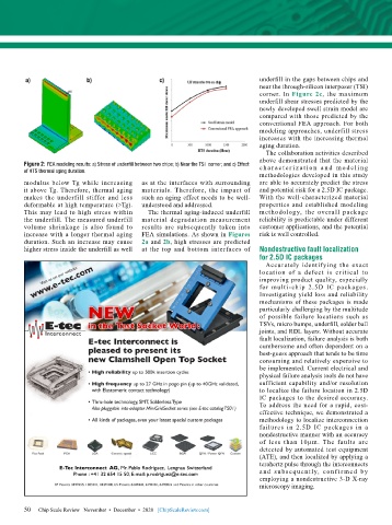
underfill in the gaps between chips and
                                                                              near the through-silicon interposer (TSI)
                                                                              corner. In  Figure 2c, the maximum
                                                                              underfill shear stresses predicted by the
                                                                              newly developed swell strain model are
                                                                              compared with those predicted by the
                                                                              conventional FEA approach. For both
                                                                              modeling approaches, underfill stress
                                                                              increases with the increasing thermal
                                                                              aging duration.
                                                                                The collaboration activities described
                                                                              above demonstrated that the material
        Figure 2: FEA modeling results: a) Stress of underfill between two chips; b) Near the TSI  corner; and c) Effect   c h a r ac t er i z a t i o n  a n d  m o d e li n g
        of HTS thermal aging duration.
                                                                              methodologies developed in this study
        modulus below Tg while increasing   as at the interfaces with surrounding   are able to accurately predict the stress
        it above Tg. Therefore, thermal aging   materials. Therefore, the impact of   and potential risk for a 2.5D IC package.
        makes the underfill stiffer and less   such an aging effect needs to be well-  With the well-characterized material
        deformable at high temperature (>Tg).   understood and addressed.     properties and established modeling
        This may lead to high stress within   The thermal aging-induced underfill   methodology, the overall package
        the underfill. The measured underfill   material  degradation  measurement   reliability is predictable under different
        volume  shrinkage  is  also  found  to   results are subsequently taken into   customer applications, and the potential
        increase with a longer thermal aging   FEA simulations. As shown in Figures   risk is well controlled.
        duration. Such an increase may cause   2a and 2b, high stresses are predicted
        higher stress inside the underfill as well   at the top and bottom interfaces of   Nondestructive fault localization
                                                                              for 2.5D IC packages
                                                                                Accurately identifying the exact
                                                                              location of a defect is critical to
                                                                              improving product quality, especially
                                                                              for  multi-chip  2.5D  IC  packages.
                                                                              Investigating yield loss and reliability
                                                                              mechanisms of these packages is made
                                                                              particularly challenging by the multitude
                                                                              of possible failure locations such as
                                                                              TSVs, micro bumps, underfill, solder ball
                                                                              joints, and RDL layers. Without accurate
                                                                              fault localization, failure analysis is both
                                                                              cumbersome and often dependent on a
                                                                              best-guess approach that tends to be time
                                                                              consuming and relatively expensive to
                                                                              be implemented. Current electrical and
                                                                              physical failure analysis tools do not have
                                                                              sufficient capability and/or resolution
                                                                              to localize the failure location in 2.5D
                                                                              IC packages to the desired accuracy.
                                                                              To address the need for a rapid, cost-
                                                                              effective technique, we demonstrated a
                                                                              methodology to localize interconnection
                                                                              failures in 2.5D IC packages in a
                                                                              nondestructive manner with an accuracy
                                                                              of  less  than  10μm.  The  faults  are
                                                                              detected by automated test equipment
                                                                              (ATE), and then localized by applying a
                                                                              terahertz pulse through the interconnects
                   E-Tec Interconnect  AG, Mr. Pablo Rodriguez,  Lengnau Switzerland  a nd subsequently, con f i r med by
                       Phone : +41 32 654 15 50, E-mail: p.rodriguez@e-tec.com
                                                                              employing a nondestructive 3-D X-ray
                                                                              microscopy imaging.


        50   Chip Scale Review   November  •  December  •  2020   [ChipScaleReview.com]
        50

