Page 10 - Chip Scale Review_January-February_2024-digital
P. 10
Two distinct approaches have been
        considered for controlling bonding
        fingerprints. The first relies exclusively
        on the actuation capability of the bonding
        tool, while the second requires concurrent
        actuation by both the bonding tool and the
        lithography scanner. The overlays resulting
        from these approaches are called “post-
        bond overlay” when exclusively achieved
        with the bonding equipment, and “post-litho
        overlay” when lithography correction is
        also needed.

        Wafer bonding optimization
          The intricate understanding of bond
        wave propagation and its influence on
        overlay underscores its strong dependence
        on  various  factors,  encompassing
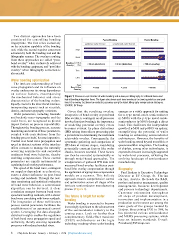
        the mechanical behavior and stress   Figure 1: Process co-optimization of wafer bonding and subsequent lithography for different fusion and
        characteristics of the bonding wafers.   hybrid bonding integration flows. The figure also shows post-bond overlay at the bonding interface and post-
        Equally crucial is the direct bond interface,   bond litho overlay that describe contacting accuracy using the latest lithography compensation strategies.
        incorporating aspects such as via pitch,   SOURCE: EV Group
        density, and nano topography variations.   Given that the resulting overlay,   emerges as a viable approach for uniting
          Wafer parameters, including frontside   irrespective of bond overlay or post-bond   the n-type metal-oxide-semiconductor
        and backside nano topography and the   litho overlay, is contingent on all processes   (n-MOS) with the p-type metal-oxide-
        wafer bevel, are recognized as pivotal   involved (not just bonding), the importance   semiconductor (p-MOS) through a direct
        impact factors on process repeatability.   of modeling potential overlay errors   bond. This facilitates the independent
        Throughout the bonding process, accurate   becomes evident. In-plane distortions   growth of n-MOS and p-MOS via epitaxy,
        monitoring and control of these parameters,   (IPD) arising from silicon processing play   exemplifying the potential of wafer
        coupled with contributions from the   a pivotal role in determining the maximum   bonding in enhancing semiconductor
        bonding process itself, become imperative.   achievable overlay. Consequently, the   architectures. However, the benefits of
        Control over bond wave propagation and   systematic gathering and comparison of   wafer bonding extend beyond monolithic or
        speed in distinct sections of the interface   IPD data at various stages, considering   quasi-monolithic integration. The bonding
        offers a means to manage the naturally   potentially constant factors like wafer   of chiplets, among other technologies, is
        occurring asymmetric and somewhat   chucks, becomes essential. These factors   expected to become increasingly supported
        nonlinear bond wave behavior, thereby   can then be corrected systematically or   by wafer-level processes, reflecting the
        enabling compensation. These control   through model-based approaches. The   evolving landscape of semiconductor
        parameters are equally instrumental in   amalgamation of gathered IPD data with   manufacturing.
        regulating local overlay performance.  measured bond overlay facilitates post-
          The speed of the bond wave, contingent   bond litho overlay compensation through   Biography
        on angular-dependent acceleration,   the application of appropriate compensation   Paul Lindner is Executive Technology
        exerts a direct influence on post-bond   models on a scanner. This holistic   Director at EV Group, St. Florian
        scaling and residuals. Through the real-  approach ensures comprehensive control   am Inn, Austria. He heads the R&D,
        time monitoring and statistical evaluation   and optimization across all stages of the   product and project management, quality
        of bond wave behavior, a correctional   intricate semiconductor manufacturing   management, business development
        algorithm can  be  devised. A  clear   process (Figure 1).            and process technology departments.
        correlation emerges between bond wave                                 Customer orientation th roughout
        speed and resulting residuals, with a slower   The future is bright for wafer   all steps of product development,
        bond wave correlating with lower residuals.                           innovation  and  implementation  in  a
        The integration of these well-known   bonding                         production environment are among the
                                             Wafer bonding is expected to become
        process control parameters facilitates the   increasingly significant to the advancement   main goals of the groups headed by
        establishment of an automated control   of the semiconductor industry in the   Lindner. Since joining EVG in 1988, he
        system. Leveraging live data alongside   coming years. Look no further than   has pioneered various semiconductor
        statistical insights enables the regulation   complementary field-effect transistor   and MEMS processing systems, which
        of both bond wave propagation speed and   (CFET) architectures on the logic   have set industry standards. E-mail:
        uniformity, thereby ensuring repeatable   technology roadmap where wafer bonding   P.Lindner@EVGroup.com
        processes with reduced residual stress.

        8 8  Chip Scale Review   January  •  February  •  2024   [ChipScaleReview.com]

