Page 39 - Chip Scale Review_January February_2022-digital
P. 39
A 2.2D die-last integrated substrate for heterogeneous


        integration applications


        By Dyi-Chung Hu  [SiPlus Co.]
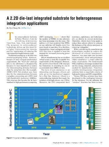
        T        he semiconductor industry   (HPC) packaging. Figure 1 shows that   resistance, capacitance, and inductance


                 follows  Moore’s  Law  by
                                           has been increasing over the years. The
                                                                              Therefore, efforts have been made to
                 sh r i n k i n g d i m e n s i o n s   the number of HBMs on one substrate   [2], as shown in circuit modeling.
        from 5nm, 3nm, 2nm, and beyond.    authors in [1] have predicted that HBMs   reduce these adverse effects by reducing
        T h e p r og r e s s i n s e m ic o n d u c t o r   on one substrate will double every five   the thickness of the silicon interposer, or
        technology drives up the need for   years based on past data. It is, therefore,   removing it altogether.
        a higher intercon nection densit y   expected that a larger packaging substrate   When considering the manufacturing
        and the requirement of reducing the   with fine lines is needed to meet the   technologies needed to reduce the
        interconnection length between chips.  demand for increased processing power   thick ness of silicon inter posers,
          Traditional packaging is divided into   in the future.              however, one must take into account
        several packaging levels. However,   Silicon manufacturing has an excellent   environmental, social and governance
        because of more stringent performance   infrastructure to meet the acceptable line   (ESG) compliance—a major effort by
        requirements, the “level one” package   requirements of the interposer. However,   many corporations. The trend toward
        (die to the substrate) is disappearing   the current silicon-based 2.5D structure   ESG compliance encourages products that
        because it’s more beneficial to reduce   has limitations in extending its size to   use less energy, materials, and processes
        the interconnecting distance between   accommodate more HBMs on time.   needed for manufacture. Therefore,
        chips by using bare dies. For example,   The term silicon interposer is an   suitable heterogeneous integration
        AMD’s  2016  Fiji  product  uses  bare   interesting one because silicon can   solutions have to meet both criteria of
        dies for the interconnection between   only act as the mechanical support   high performance and ESG compatibility.
        a graphics processing unit (GPU) and   for a fine line. However, silicon is a   Various TSV-less solutions have been
        high-bandwidth memories  (HBMs).   semiconducting material that needs the   developed in the packaging industry
        This structure has become the de facto   isolation of through-silicon vias (TSVs).   for the interposer. For the substrate, the
        standard for high-performance computing   Moreover, the TSV components have   “coreless” structure has been in mass


        Figure 1: The number of HBMs on a substrate doubles every five years.

                                                                                                             37
                                                          Chip Scale Review   January  •  February  •  2022   [ChipScaleReview.com]  37

