Page 41 - Chip Scale Review_January February_2022-digital
P. 41
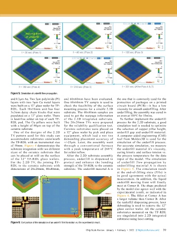
Figure 5: Simulation of underfill flow propagation.
        and 0.3µm Au. Two 5µm polyimide (PI)   and 60x60mm have been evaluated.   the one that is commonly used for the
        layers with two 3µm Cu metal layers   One 60x60mm TV sample is used to   protection of packages on a printed
        were built on a 12” glass wafer for TF-  check the feasibility of the surface   circuit board (PCB)—it has a low
        RDL. Each 10x10mm unit has four    mounting process for a sizable 2.2D   viscosity for smooth underfilling. After
        3x3mm daisy chain blocks that were   substrate. The 40x40mm samples are   underfilling, the assembly was cured in
        populated on a 12” glass wafer. There   used to get the warpage information   an oven at 150ºC for 15mins.
        is lead-free solder on top of each TF-  of the 2.2D integrated substrate.   To further implement the underfill
        RDL pad. The Cu pillars were built   The 20x20mm TVs were prepared    process for the 2.2D substrate, a good
        with a height of 80μm on top of the   for the reliability qualification test.   simulation tool is needed to optimize
        ceramic substrate                  Ceramic substrates were placed on   the selection of copper pillar height,
          One of the designs of the 2.2D   a 12” glass wafer by pick and place   underfill gap and underfill material.
        TV pattern used for this study can   equ ipment, wh ich ha d a not too   A computer aided engineering (CAE)
        accommodate substrates underneath   demanding placement accuracy of    tool from Moldex3D is used for the
        the TF-RDL with an incremental size   +/-25µm. Later, the assembly went   simulation of the underfill process.
        of 10mm. Figure 4 demonstrates the   t h roug h a conve nt ion al  f u r n a ce   For accurate simulation, we measure
        substrate integration with two different   with a peak temperature of 260ºC    the underfill material A’s viscosity,
        sizes  of the  ceramic substrate  that   for solder reflow.           curing kinetic and surface tension vs.
        can be placed at will on the surface   After the 2.2D substrate assembly   the process temperature for the data
        of the 12” TF-R DL glass wafers.   process, underfill is dispensed to   input of the model. The simulation
        For the 2.2D TV, the joining TF-   protect and enhance the bonding    of underf ill f low  propagation  by
        RDL  to  the  ceramic  substrate  with   strength of the TF-RDL to the ceramic   underf illing material A is shown
        dimensions of 20x20mm, 40x40mm,    substrate. The underfill material A is   in  Figure 5. The simulation result
                                                                              at the end-of-filling state (351s) is
                                                                              in good agreement with the actual
                                                                              measurement. In addition, the liquid
                                                                              underfill moving front will finally
                                                                              meet at Corner B. The shape predicted
                                                                              by the model also agrees well with the
                                                                              experimental result, as indicated in
                                                                              Figure 6. The fillet at Corner A has
                                                                              a larger volume than Corner B. After
                                                                              the underfill dispensing process, laser
                                                                              debonding is used to remove the 12”
                                                                              glass carrier wafer. All the ceramic
                                                                              substrates mounted on the TF-RDL
                                                                              are singulated into 2.2D integrated
                                                                              substrates using laser cutting.
        Figure 6: Comparison of the simulation of an underfill fillet formation vs. the experimental result.

                                                                                                             39
                                                          Chip Scale Review   January  •  February  •  2022   [ChipScaleReview.com]  39

