Page 42 - Chip Scale Review_January February_2022-digital
P. 42
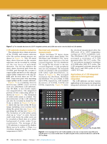
Figure 7: a) The schematic structures of a 2.2D TV integrated substrate; and b) SEM cross-section view of a 20x20mm 2.2D substrate.
        2.2D substrate structure evaluation  Electrical and reliability       the electrical measurement after the
          The schematic daisy chain structures   measurements                 1000-cycle -65 to +150ºC temperature
        of the TF-RDL and ceramic substrate   Each 10x10mm TV daisy chain     cycling test (TCT) (reliability test).
        after the surface mount process are   unit has four daisy chain blocks. For   The 20x20mm 2.2D TV test pattern
        shown in  Figure 7a. This 3D metal   20x20mm and 40x40mm TVs, daisy   ave r a ge d  a  r e si s t a n c e  of  0. 38 Ω
        daisy chain structure on the ceramic   chain blocks are measured in the two   measured after 500 TCT cycles. The
        substrate can be revealed by etching   crossed diagonals. For the 60x60mm   TV test pattern averaged a resistance
        of f t he t wo laye r s of poly i m ide   TV, except for the blocks in the two   of 0.386Ω after 1000 TCT cycles. The
        dielectric. The red line indicates the   crossed diagonals, 4-side peripheral   2.2D integrated substrate passed the
        daisy chain electrical path from the   ones are also measured. The measured   MSL level 4 and 1000 cycles of -65 to
        TF-RDL  pad  through  the  ceramic’s   results are plotted in the accumulation   +150ºC TCT test.
        copper pillar and moves to the adjacent   with rather tight distributions, as
        copper pillar connected to the top TF-  shown in  Figure 9a. The averaged   Applications of a 2.2D integrated
        RDL pad. In total, there are 7x7 TF-  resistances for 20x20mm, 40x40mm   substrate to heterogeneous
        RDL connection pads with matching   and 60x60mm TVs are 0.366Ω, 0.336Ω   integration
        copper pillars on the ceramic substrate.  and 0.347Ω, respectively, with standard   The 2.2D substrate can have various
          Figure 7b is a scanning electron   deviations  of  0.035Ω,  0.027Ω  and   applications as heterogeneous integration
        microscope (SEM) cross-section     0.021Ω, respectively. Figure 9b shows   integrated substrates for mid-end and
        view of a 20x20mm 2.2D substrate.
        The TF-R DL is not visible under
        this magnification. The magnified
        portion of two connecting pillars is
        shown in  Figure 7c. The formation
        of solid solder joints is evident. The
        microstructure of the 2.2D substrate
        can also be revealed in detail by 3D
        X-ray as shown in Figure 8. Figure
        8a shows the top view of the 3D X-ray
        image including cross-section views
        along the green line (see Figure 8b)
        and along the red line (see Figure 8c).
        The formation of solid solder joints
        show up as “clear” in color. Several
        small voids inside the solder joint can
        be revealed as black dots on a white
        background of solder under X-ray
        examination. The war page of the
        2.2D substrate is measured by shadow
        Moiré test to be within +/-20μm in a
        40x40mm diagonal range from room
        temperature to 260ºC.              Figure 8: A 3D X-ray image of the 2.2D TV after assembly: a) Top view; b) Cross-section view of the joints
                                           along the green line; c) Cross-section view of the joints along the red line; and d) An Xradia 520 is used for the
                                           3D X-ray image.

        40   Chip Scale Review   January  •  February  •  2022   [ChipScaleReview.com]
        40

