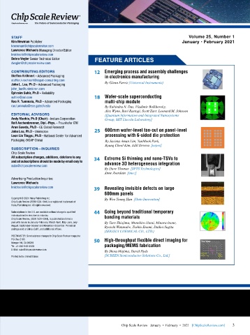
Page 5 - ChipScale_Jan-Feb_2021-digital
P. 5
The Future of Semiconductor Packaging


      STAFF                                                                              Volume 25, Number 1
      Kim Newman Publisher                                                            January • February 2021
      knewman@chipscalereview.com
      Lawrence Michaels Managing Director/Editor
      lmichaels@chipscalereview.com
      Debra Vogler Senior Technical Editor      FEATURE ARTICLES
      dvogler@chipscalereview.com
      CONTRIBUTING EDITORS                   12   Emerging process and assembly challenges
      Steffen Kröhnert - Advanced Packaging       in electronics manufacturing
 DIE-TO-WAFER (D2W)  steffen.kroehnert@espat-consulting.com  By Glenn Farris [Universal Instruments]
      John L. Lau, Ph.D - Advanced Packaging
      john_lau@unimicron.com
 BONDING SOLUTIONS  Ephraim Suhir, Ph.D - Reliability  18  Wafer-scale superconducting
      suhire@aol.com
                                                  multi-chip module
      Rao R. Tummala, Ph.D - Advanced Packaging
      rao.tummala@ece.gatech.edu                  By Rabindra N. Das, Vladimir Bolkhovsky,
                                                  Alex Wynn, Ravi Rastogi, Scott Zarr, Leonard M. Johnson
      EDITORIAL ADVISORS                          [Quantum Information and Integrated Nanosystems
      Andy Mackie, Ph.D (Chair) - Indium Corporation  Group, MIT Lincoln Laboratory]
      Rolf Aschenbrenner, Dipl.-Phys. - Fraunhofer IZM
      Arun Gowda, Ph.D - GE Global Research
      John Lau, Ph.D - Unimicron             25   600mm wafer-level fan-out on panel-level
      Leon Lin Tingyu, Ph.D - National Center for Advanced   processing with 6-sided die protection
      Packaging (NCAP China)                      By Jacinta Aman Lim, YunMook Park,
 Fusion and hybrid bonding for next-generation  SUBSCRIPTION—INQUIRIES  Byung Cheol Kim, Edil Devera  [nepes]
 heterogeneous integration  Chip Scale Review
      All subscription changes, additions, deletions to any   34  Extreme Si thinning and nano-TSVs to
      and all subscriptions should be made by email only to     advance 3D heterogeneous integration
 Collective D2W bonding enabled by extensive  subs@chipscalereview.com  By Dave Thomas  [SPTS Technologies]
 knowledge in carrier preparation and die handling  Anne Jourdain  [imec]
      Advertising Production Inquiries:
      Lawrence Michaels
 Direct placement D2W activation and cleaning  lmichaels@chipscalereview.com  39  Revealing invisible defects on large
 complete solution with EVG®320 D2W  Copyright © 2021 Haley Publishing Inc.  600mm panels
                                                  By Woo Young Han  [Onto Innovation]
      Chip Scale Review (ISSN 1526-1344) is a registered trademark of
      Haley Publishing Inc. All rights reserved.
 Production-ready equipment solutions for  Subscriptions in the U.S. are available without charge to qualified  44  Going beyond traditional temporary
 successful integration of chiplets  individuals in the electronics industry.   bonding materials
      Chip Scale Review, (ISSN 1526-1344), is published six times a
      year with issues in January-February, March-April, May-June, July-  By Taro Shiojima, Munehiro Hatai, Minoru Inoue,
      August, September-October and November-December. Periodical  Ryoichi Watanabe, Toshio Enami, Daihei Sugita
      postage paid at Gilroy, Calif., and additional offices.
 Heterogeneous Integration Competence Center™  POSTMASTER: Send address changes to Chip Scale Review magazine  [SEKISUI CHEMICAL CO., LTD.]
 serving as leading-edge incubation center  P.O. Box 2165  50  High-throughput flexible direct imaging for
      Morgan Hill, CA 95038
 for customers and partners  Tel: +1-408-846-8580  packaging/MEMS fabrication
      E-Mail: subs@chipscalereview.com
                                                  By Shota Majima, David Hyde
                                                  [SCREEN Semiconductor Solutions Co., Ltd.]
      Printed in the United States


 GET IN TOUCH to discuss your manufacturing needs
 www.EVGroup.com  EVG® 320 D2W
                                                          Chip Scale Review   January  •  February  •  2021   [ChipScaleReview.com]  3 3

