Page 8 - ChipScale_Sep-Oct_2020-digital
P. 8
provide these details, along with the   and BGA spheres, and a PCB with a short   In conclusion, socket suppliers provide
        pin-out map, in partnering with socket   via transition on the top and simulated the   specification sheets for socket and pin
        suppliers in the development of the   same structure to validate the model. An   families to provide customers a way of
        socket technology in order to achieve   example of the new simulation set-up used   comparing one design to another. These
        the best possible system performance.   to validate the measurement is shown in   specifications should only be considered
        When the socket designer develops a   Figure 3. The simulation and measured   as  a  reference  point  in making  an
        customer solution, a design standard   results match very well as shown in the   initial decision on the preferred socket
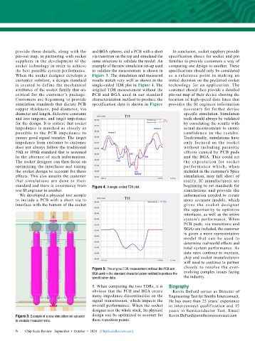
        is created to define the mechanical   single-ended TDR plot in Figure 4. The   technology for an application.  The
        attributes of the socket family that are   original TDR measurement without the   customer should then provide a detailed
        critical for the customer’s package.   PCB and BGA used in our standard   pin-out map of their device showing the
        Customers are beginning to provide   characterization method to produce the   location of high-speed data lines that
        simulation standards that dictate PCB   specification data is shown in Figure   provides the SI engineer information
        copper thickness, pad diameter, via                                          necessary for further device
        diameter and length, dielectric constants                                    specific simulation. Simulation
        and loss tangents, and target impedance                                      tools should always be validated
        for the design. It is critical that socket                                   by correlating the results with
        impedance is matched as closely as                                           actual measurements to ensure
        possible to the PCB impedance to                                             conf idence  in  the  results.
        ensure good signal transfer. The target                                      Traditionally, simulations have
        impedance from customer to customer                                          only focused on the socket
        does not always follow the traditional                                       without including parasitic
        50Ω or 100Ω standard that is assumed                                         effects  caused  by PCB pads
        in the absence of such information.                                          and the BGA. This could set
        The socket designer can then focus on                                        the expectation for socket
        optimizing the interfaces and tuning                                         perfor mance which, when
        the socket design to account for these                                       included in the customer’s Spice
        effects. This also assures the customer                                      simulation, may fall short of
        that simulations are done to their                                           reality. IC manufacturers are
        standard and there is consistency from   Figure 4: A single-ended TDR plot.  beginning to set standards for
        one SI engineer to another.                                                  simulations and provide the
          We developed a physical test sample                                        information needed to create
        to include a PCB with a short via to                                         more accurate models, which
        interface with the bottom of the socket                                      gives the socket desig ner
                                                                                     the opportunity to optimize
                                                                                     interfaces, as well as the entire
                                                                                     system’s performance. When
                                                                                     PCB pads, via transitions and
                                                                                     BGAs are included, the customer
                                                                                     is given a more representative
                                                                                     model that can be used to
                                                                                     determine real-world effects and
                                                                                     total system performance. As
                                                                                     data rates continue to increase,
                                                                                     chip and socket manufacturers
                                                                                     will need to continue to partner
                                                                                     closely to resolve the ever-
                                           Figure 5: The original TDR measurement without the PCB and
                                           BGA used in the standard characterization method to produce the   evolving complex issues facing
                                           specification data.                       the industry.
                                           5. When comparing the two TDRs, it is   Biography
                                           obvious that the PCB and BGA create   Kevin DeFord serves as Director of
                                           many impedance discontinuities on the   Engineering Test for Smiths Interconnect.
                                           signal transmission, which impacts the   He has more than 25 years’ experience
                                           overall performance. When the socket   in interconnect qualification and 15
                                           designer sees the whole stack, the physical   years in Semiconductor Test. Email
        Figure 3: Example of a new simulation set-up used   design can be optimized to account for   Kevin.DeFord@smithsinterconnect.com
        to validate measurements.          these transition points.

        6 6  Chip Scale Review   September  •  October  •  2020   [ChipScaleReview.com]

