Page 43 - Chip Scale Review_Jul Aug_2022-digital
P. 43
posed by putting more electronic content
                                                                             into smaller spaces and supporting the
                                                                             development of flexible electronics, including
                                                                             large-area displays. Recent developments in
                                                                             silicone technology can address these and
                                                                             other packaging challenges, and advanced
                                                                             silicones can complement rather than replace
                                                                             epoxies by providing an effective wafer-level
                                                                             solution.

                                                                             Biography
                                                                               Jayden Cho is Global Segment Leader at
                                                                             Dow, Korea. His career spans 18 years in
                                                                             silicones for electronics, acrylic industrial
                                                                             tapes (PSAs) for electronics, and silicones
                                                                             for the building industry. He holds a
                                                                             Bachelor’s degree in Polymer Science
                                                                             Engineering from Dankook U., Korea.
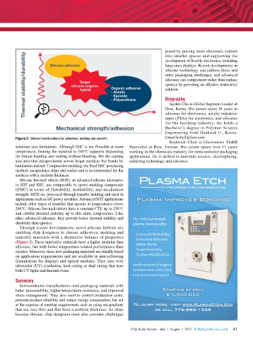
        Figure 2: Silicone hybrid options for adhesives, molding and underfill.  Email kcho2@dow.com
                                                                               Roderick Chen is Electronics TS&D
        substrate size limitations. Although SHC is not flowable at room   Specialist at Dow, Taiwan. His career spans over 13 years
        temperature, heating the material to 100°C supports dispensing   working in the chemicals industry for semiconductor packaging
        for instant bonding and sealing without bleeding. Slit die coating   applications. He is skilled in materials science, electroplating,
        also provides encapsulation across larger surfaces but bonds by   soldering technology and silicones.
        lamination instead. Compression molding, the third SHC processing
        method, encapsulates chips and wafers and is recommended for flat
        surfaces with a uniform thickness.
          Silicone hot-melt tablets (SHT), an advanced silicone alternative
        to SHF and SHC, are comparable to epoxy molding compounds
        (EMC) in terms of flowability, moldability, and mechanical
        strength. SHTs are processed through transfer molding and used in
        applications such as IoT power modules. Advanced SHT applications
        include other types of modules that operate at temperatures above
        200°C. Silicone hot-melt tablets have a constant CTE up to 250°C
        and exhibit thermal stability up to this same temperature. Like
        other advanced silicones, they provide better thermal stability and
        durability than epoxies.
          Through recent developments, novel silicone hybrids are
        enabling chip designers to choose adhesives, molding and
        underfill materials with a distinctive balance of properties
        (Figure 2). These innovative materials have a higher modulus than
        silicones, but with better temperature-related performance than
        epoxies. Moreover, these new packaging materials are tunable based
        on application requirements and are available in non-yellowing
        formulations for displays and optical modules. They cure with
        ultraviolet (UV) irradiation, heat curing or dual curing that uses
        both UV lights and thermal ovens.

        Summary
          Semiconductor manufacturers need packaging materials with
        better processability, higher-temperature resistance, and improved
        stress management. They also want to control production costs,
        promote product reliability and reduce energy consumption, but not
        at the expense of meeting requirements such as using encapsulants
        that are very thin and that have a uniform thickness. As chips
        become thinner, chip designers must also consider challenges


                                                                                                             41
                                                             Chip Scale Review   July  •  August  •  2022   [ChipScaleReview.com]  41

