Page 33 - Chip Scale Review_January February_2022-digital
P. 33
exposure limit (currently  33mm x 26mm
                2
        = 858mm ; the IEEE IRDS chapter on
        lithography [9] has projected trends).
        However, the maximum practical size of
        a commercial volume chip will still be
        limited by thermal, mechanical warpage,
        etc., considerations.
          Chiplets can also help reduce project
        costs, scale innovation and delivery
        capabilities, and reduce time to solution.
        Ideally, chiplets would largely be reusable
        within and between product/solution
        generations and product lines while
        supporting per segment and potentially
        per customer feature tailoring where it is
        desired. For example, a chiplet approach
        would  help a  hyperscalar  deploy  a
        particular and potentially proprietary type
        of machine learning accelerator uniformly
        (albeit perhaps at different performance
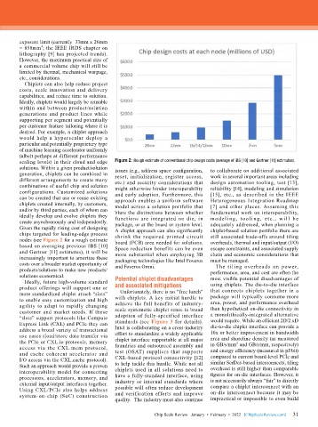
        scaling levels) in their cloud and edge   Figure 2: Rough estimate of conventional chip design costs (average of IBS [10] and Gartner [11] estimates).
        solutions. Within a given product/solution   issues (e.g., address space configuration,   to collaborate on additional associated
        generation, chiplets can be combined in   reset, initialization, register access,   work in several important areas including
        different arrangements to create many   etc.) and security considerations that   design automation tooling, test [13],
        combinations of useful chip and solution   might otherwise hinder interoperability   reliability [14], modeling and simulation
        configurations. Customized solutions   and early adoption. Furthermore, this   [15], etc., as described in the IEEE
        can be created that use or reuse existing   approach enables a uniform software   Heterogeneous Integration Roadmap
        chiplets created internally, by customers,   model across a solution portfolio that   [7] and other places. Assuming this
        and/or by third parties, each of whom can   blurs the distinctions between whether   fundamental work on interoperability,
        ideally develop and evolve chiplets they   functions are integrated on die, in   model i ng, t ool i ng, et c., w il l be
        create asynchronously and independently.   package, or at the board or system level.   adequately addressed, when planning a
        Given the rapidly rising cost of designing   A chiplet approach can also significantly   chiplet-based solution portfolio there are
        chips targeted for leading-edge process   shrink the required printed circuit   still associated trade-offs around tiling
        nodes (see Figure 2 for a rough estimate   board (PCB) area needed for solutions.   overheads, thermal and input/output (I/O)
        based on averaging previous IBS [10]   Space reduction benefits can be even   escape constraints, and associated supply
        and Gartner [11] estimates), it will be   more substantial when employing 3D   chain and economic considerations that
        increasingly important to amortize these   packaging technologies like Intel Foveros   must be managed.
        costs over a broader market opportunity of   and Foveros Omni.          The tiling overheads on power,
        products/solutions to make new products/                              performance, area, and cost are often the
        solutions economical.                                                 most visible potential disadvantages of
          Ideally, future high-volume standard   Potential chiplet disadvantages   using chiplets. The die-to-die interface
        product offerings will support one or   and associated mitigations    that connects chiplets together in a
        more standardized chiplet attach “slots”   Unfortunately, there is no “free lunch”   package will typically consume more
        to enable easy customization and high   with chiplets. A key initial hurdle to   area, power, and performance overhead
        agility to adapt to rapidly changing   achieve the full benefits of industry-  than hypothetical on-die connectivity in
        customer and market needs. If these   scale systematic chiplet reuse is broad   a monolithically-integrated alternative
        “slots” support protocols like Compute   adoption of fully-specified interface   would require. While an efficient 2D/2.xD
        Express Link (CXL) and PCIe they can   standards (see Figure 3 for details).   die-to-die chiplet interface can provide a
        address a broad variety of transactional   Intel is collaborating on a cross-industry   10x or better improvement in bandwidth
        use cases (load/store data transfer via   effort to standardize a widely applicable   area and shoreline density (as measured
        the PCIe or CXL.io protocols, memory   chiplet interface supportable at all major   in GB/s/mm  and GB/s/mm, respectively)
                                                                                        2
        access via the CXL.mem protocol,   foundries and outsourced assembly and   and energy efficiency (measured in pJ/bit)
        and cache coherent accelerator and    test  (OSAT) suppliers that supports   compared to current board-level PCIe and
        I/O access via the CXL.cache protocol).   CXL-based protocol connectivity [12]   similar SerDes-based interconnects, tiling
        Such an approach would provide a proven   to help tackle this hurdle. While not all   overhead is still higher than comparable
        interoperability model for connecting   chiplets used in all solutions need to   figures for on-die interfaces. However, it
        processors, accelerators, memory, and   have a fully-standard interface, using   is not necessarily always “fair” to directly
        external input/output interfaces together.   industry or internal standards where   compare a chiplet interconnect with an
        Using CXL/PCIe also helps address   possible will often reduce development   on-die interconnect because it may be
        system-on-chip (SoC) construction   and verification efforts and improve
                                           quality.  The industry must also continue   impractical or impossible to even build

                                                                                                             31
                                                          Chip Scale Review   January  •  February  •  2022   [ChipScaleReview.com]  31

