Page 45 - ChipScale_Nov-Dec_2020-digital
P. 45
Functionalized materials enable yield improvement in


        package test


        By Jerry Broz, Bret Humphrey  [International Test Solutions, Inc.]
        A         pplication demands are


                  bei ng d r iven by major
                  technological megatrends in
        personal devices, data cloud, connectivity,
        and automotive content. Additionally,
        Moore’s Law is slowing, so semiconductor
        manufacturers are pursuing heterogeneous
        integration strategies that combine the
        benefits of multiple processors, memory
        modules, and other intellectual property
        (IP) from different nodes and various
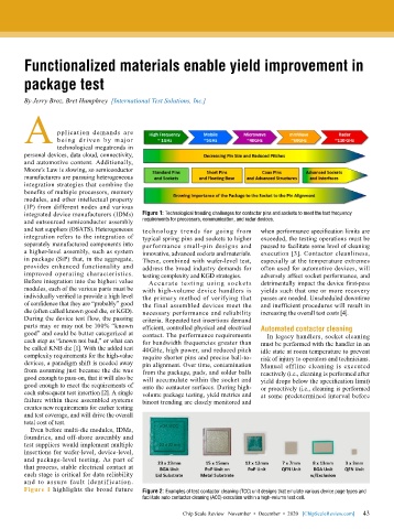
        integrated device manufacturers (IDMs)   Figure 1: Technological trending challenges for contactor pins and sockets to meet the test frequency
        and outsourced semiconductor assembly   requirements for processors, communication, and radar devices.
        and test suppliers (OSATS). Heterogeneous   technology trends for going from   when performance specification limits are
        integration refers to the integration of   typical spring pins and sockets to higher   exceeded, the testing operations must be
        separately manufactured components into   performance small-pin designs and   paused to facilitate some level of cleaning
        a higher-level assembly, such as system   innovative, advanced sockets and materials.   execution [3]. Contactor cleanliness,
        in package (SiP) that, in the aggregate,   These, combined with wafer-level test,   especially at the temperature extremes
        provides enhanced functionality and   address the broad industry demands for   often used for automotive devices, will
        improved operating characteristics.   testing complexity and KGD strategies.  adversely affect socket performance, and
        Before integration into the highest value   Accurate testing using sockets   detrimentally impact the device first-pass
        modules, each of the various parts must be   with high-volume device handlers is   yields such that one or more recovery
        individually verified to provide a high level   the primary method of verifying that   passes are needed. Unscheduled downtime
        of confidence that they are “probably” good   the final assembled devices meet the   and inefficient procedures will result in
        die (often called known good die, or KGD).   necessary performance and reliability   increasing the overall test costs [4].
        During the device test flow, the passing   criteria. Repeated test insertions demand
        parts may or may not be 100% “known   efficient, controlled physical and electrical   Automated contactor cleaning
        good” and could be better categorized at   contact. The performance requirements   In legacy handlers, socket cleaning
        each step as “known not bad,” or what can   for bandwidth frequencies greater than   must be performed with the handler in an
        be called KNB die [1]. With the added test   40GHz, high power, and reduced pitch   idle state at room temperature to prevent
        complexity requirements for the high-value   require shorter pins and precise ball-to-  risk of injury to operators and technicians.
        devices, a paradigm shift is needed away   pin alignment. Over time, contamination   Manual offline cleaning is executed
        from assuming just because the die was   from the package, pads, and solder balls   reactively (i.e., cleaning is performed after
        good enough to pass-on, that it will also be   will accumulate within the socket and   yield drops below the specification limit)
        good enough to meet the requirements of   onto the contactor surfaces. During high-  or proactively (i.e., cleaning is performed
        each subsequent test insertion [2]. A single   volume package testing, yield metrics and   at some predetermined interval before
        failure within these assembled systems   binout trending are closely monitored and
        creates new requirements for earlier testing
        and test coverage, and will drive the overall
        total cost of test.
          Even before multi-die modules, IDMs,
        foundries, and off-shore assembly and
        test suppliers would implement multiple
        insertions for wafer-level, device-level,
        and package-level testing. As part of
        that process, stable electrical contact at
        each stage is critical for data reliability
        and to assure fault identification.
        Figure 1 highlights the broad future   Figure 2: Examples of test contactor cleaning (TCC) unit designs that emulate various device page types and
                                           facilitate auto contactor cleaning (ACC) execution within a high-volume test cell.

                                                                                                             43
                                                       Chip Scale Review   November  •  December  •  2020   [ChipScaleReview.com]  43

