Page 57 - Chip Scale Review_January February_2022-digital
P. 57
mode fiber,” Jour. of Lightwave
                                                                                  Tech., 2015 | Vol. 33, Issue: 6.
                                                                                2. Y. Ya ng, M. Yu , Q. Fa ng, J.
                                                                                  Song, X. Tu, P. G-Q. Lo, et al.,
                                                                                  “3D silicon photonics packaging
                                                                                  based on TSV interposer for high-
                                                                                  density on-board optics module,“
                                                                                  2016 IEEE 66th Elec. Comp. and
                                                                                  Tech. Conf. (ECTC).
                                                                                3. T G. Lim, D. S. W. Ho, E. W. L.
                                                                                  Ching, Z. Chen, S. Bhattacharya,
                                                                                  “FOWLP design for digital and RF
                                                                                  circuits,” 2019 IEEE 69th ECTC.
                                                                                4. H . U e m u r a , K . Wa r a b i , K .
                                                                                  Ohira, Y. Kurita, H. Yoshida,
                                                                                  H. Furuyama, et al., “Backside
                                                                                  o pt i c a l  I / O mo d u l e  f o r  S i
                                                                                  p ho t o n i c s i n t e g r a t e d w i t h
                                                                                  electrical ICs using fan-out wafer-
                                                                                  level packaging technology,” 2018
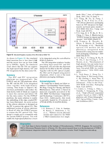
        Figure 12: Simulated frequency response of the differential (or GSSG) TSV.  IEEE 68th ECTC.
        As shown in Figure 12, the simulated   to be integrated using the cost-effective   5. V. S. Rao, C. T. Chong, D. Ho, D.
        ideal insertion loss is less than 0.5dB   FOWLP platform.                 M. Zhi, C. Ser Choong, L. P. S.
        and the return loss can go from 10dB   The TSI integration platform, besides   Sharon, et al., “Development of
        up to 100GHz. Again, the simulated   providing high-speed PIC and EIC     high-density fan-out wafer-level
        result shows that the TSI can support   integration, also provides the alignment   package (HD FOWLP) with multi-
        the high-speed high-density EIC and   feature for the fiber to the PIC assembly.   layer fine-pitch RDL for mobile
        PIC integration for the data center OE.  Together with the PIC optical coupler,   applications,” 2016 IEEE 66th
                                           the fiber can be aligned using passive   ECTC.
        Summary                            alignment, which is one of the main   6. L.  Teck  Guan,  L.  Hong  Yu,  J.
          Two EIC a n d PIC i nt eg r a t io n   photonics packaging challenges.  Ming Chinq, E. Wai Leong Ching,
        platforms  are  proposed  here.  The                                      C. Ser Choong, L. Soon Thor, et
        FOWLP and the TSI platforms allow   Acknowledgments                       al., “Silicon Optical Electrical
        the PIC and the EIC to be integrated   We would like to thank our fellow co-  Interposer - Fiber to the Chip,”
        close together with high-densit y   authors: Chockanathan Vinoth Kanna,   2019 IEEE 21st Elec. Packaging
        routing. This helps to improve the   Wu Jiaqi, Chong Ser Choong, and Surya   Tech. Conf. (EPTC).
        electrical performance and reduce the   Bhattacharya. This article is based on   7. J. Lianxi, L. T-Yang, L. Chao, L.
        form factor, both of which are required   materials originally presented at the   Xianshu, T. Xiaoguang, H. Ying,
        to meet the current and future OE   2021 IEEE 71st Electronic Components   et al., “High efficient suspended
        for the data center. For the FOWLP   and Technology Conference (ECTC),    coupler  based  on  IME’s  MPW
        platform, the main solution to enable   June 2021. Additionally, this work   platform with 193nm lithography,”
        the embedding of the edge-coupled PIC   is partially funded by A*ccelerate of   2017 Optical Fiber Comm. Conf.
        has been illustrated. An extra section   A*STAR (ETPL/18-GAP056-R20A).    and Exhibition (OFC).
        of the silicon substrate is designed on
        the PIC to protect the optical I/O. This   References
        additional section of silicon substrate   1. G. Denoyer, C. Cole, A. Santipo,
        is diced off after the FOWLP process   R. Russo, C. Robinson, L. Li,
        to expose the PIC optical I/Os. This   et al., “Hybrid silicon photonic
        design is simple and is compatible with   circuits and transceiver for 50Gb/
        the current FOWLP process. This will   s NRZ transmission over single-
        enable the high-speed photonics circuit


                       Biographies
                         Lim Teck Guan is Senior Scientist at the Institute of Microelectronics, A*STAR, Singapore. He received his
                       PhD in Microwave Photonics from U. of Surrey, UK. His current research focus is on the development of FOWLP
                       and Si-interposer integration solutions for mmWave and photonics circuits. Email: limtg@ime.a-star.edu.sg


                                                                                                             55
                                                          Chip Scale Review   January  •  February  •  2022   [ChipScaleReview.com]  55

