Page 53 - Chip Scale Review_January February_2023-digital
P. 53
Bougie, A. Drouin, R. Langlois,
                                                                                   et al., “Towards co-packaging  of
                                                                                   photonics  and  microelectronics  in
                                                                                   existing manufacturing  facilities,”
                                                                                   SPIE  Proc. 10538. (22  February
                                                                                   2018) 10.1117/12.2291902.
                                                                                 5.  N. Boyer, A. Janta-Polczynski, J.
                                                                                   Morissette, S. Martel, T. Lichoulas,
                                                                                   S. Kamlapurkar, et al., “Novel,
                                                                                   high-throughput, fiber-to-chip
                                                                                   assembly employing only off-the-
                                                                                   shelf components,” Proc. of IEEE
                                                                                   ECTC, New York, 2017, pp. 1632 -
                                                                                   1639.
                                                                                 6.  A. Janta-Polczynski, C. Blackburn,
                                                                                   N. Tracy,  “Co-packaged optics
                                                                                   s o c ke t s  fo r   C P O,”   O p t i c a l
                                                                                   Internetworking Forum (OIF), PLL
                                                                                   Co-packaging Working Group,
                                                                                   oif2021.181.00.
                                                                                 7.  Y. Frans, P. Upadhyaya, M. Raj,
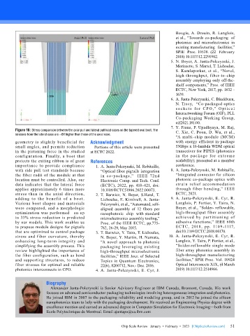
        Figure 16: Stress comparison between the axial pull and lateral pull load cases on the tapered oval boot. The   C. Xie, C. Poon, D. Wu, et al.,
        stresses from the lateral case are ~6X higher than those of the axial case.
                                                                                   “A  multi-chip  module  (MCM)
        geometry  is  slightly  beneficial  for   Acknowledgment                   with energy efficient in-package
        small angles, and permits reduction   Portions of this article were presented   53Gbps x 16-lambda WDM optical
        in the pistoning force in the studied   at ECTC 2022.                      transceiver for PIPES (photonics
        configuration.  Finally,  a  boot  that                                    i n t he pack age for ext reme
        protects the exiting ribbon is of great   References                       scalability); presented at a member
        importance  to  provide  compliance   1.  A. Janta-Polczynski, M. Robitaille,   conference.
        with side pull test standards because   “Optical fiber pigtails integration   8.  A. Janta-Polczynski, M. Robitaille,
        the fiber radii of the module at that   in  co-package,”    IEEE  72nd     “Integrated connector for silicon
        location must be controlled. Also, our   Electronic Comp. and Tech. Conf.   photonic co-package optics with
        data indicates that the lateral force   (ECTC), 2022, pp. 410-421, doi:    strain  relief  accommodation
        applies approximately 6 times more      10.1109/ECTC51906.2022.00073.      through  fiber  bending,”  IEEE
        stress than in the axial direction,   2.  T.  Barwicz,  N.  Boyer,  S.Harel,  T.     ECTC, 2021.
        add i ng to t he benef it of a boot.    Lichoulas, E. Kimbrell, A. Janta-  9.  A. Janta-Polczynski, E. Cyr, R.
        Various  boot  shapes  and  materials   Polczynski, et al., “Automated, self-  Langlois, P. Fortier, Y. Taira, N.
        were  compared,  and  a  morphologic    aligned  assembly  of  12  fibers  per    Boyer, et al., “Solder- reflowable,
        optimization was performed—an up        nanophotonic  chip  with standard   high-throughput fiber assembly
        to 33% stress reduction is predicted    microelectronics assembly tooling,”   achieved by par titioni ng of
        by our models. This work enables us     Proc. of the IEEE ECTC, pp.775-    adhesive functions,” IEEE 68th
        to propose module designs for pigtails   782, 26-29, May 2015.             ECTC, 2018, pp. 1109-1117,
        that are optimized to control package   3.  T. Barwicz, Y. Taira, T. Lichoulas,   doi:10.1109/ECTC.2018.00170.
        stress and fiber curvature, thereby     N. Boyer, Y. Martin, H. Numata,   10.  A. Janta-Polczynski, E. Cyr, R.
        enhancing  long-term  integrity  and    “A novel approach to photonic      Langlois, Y. Taira, P. Fortier, et al.,
        simplifying the assembly process. This   packaging leveraging existing     “Solder-reflowable single mode
        review highlighted the importance of    high-throughput microelectronic    fiber array photonics assembly in
        the fiber configuration, such as bend   facilities,” IEEE Jour. of Selected   high-throughput manufacturing
        and supporting structures, to reduce    Topics in Quantum Electronics,     facilities,” SPIE Proc. Vol. 10924
        fiber stresses for optimal and reliable   22(6), 8200712, Nov.- Dec. 2016.  Optical Interconects XIX, (4 March
        photonics interconnects in CPO.       4.  A. Janta-Polczynski, E. Cyr, J.   2019) 10.1117/12.2514966.


                       Biography
                         Alexander Janta-Polczynski is Senior Advisory Engineer at IBM Canada, Bromont, Canada. His work
                       focuses on advanced semiconductor packaging technologies involving heterogeneous integration and photonics.
                       He joined IBM in 2007 in the packaging reliability and modeling group, and in 2012 he joined the silicon
                       nanophotonics team to help with the packaging development. He received an Engineering Physics degree with
                       excellence mention and earned an advanced degree in Computer Simulation for Electronic Imaging—both from
                       Ecole Polytechnique de Montreal. Email ajantapo@ca.ibm.com


                                                                                                             51
                                                          Chip Scale Review   January  •  February  •  2023   [ChipScaleReview.com]  51

