Page 24 - Chip Scale Review_January February_2022-digital
P. 24
chiplets as shown in Figure 3 and TSMC
                                                                              manufactured the chiplets at high yield
                                                                              (with the 28nm process technology) and
                                                                              packaged them on their chip-on-wafer-on-
                                                                              substrate (CoWoS) technology. CoWoS
                                                                              is a 2.5D IC integration, which is the key
                                                                              structure (substrate) to let those 4 chiplets
                                                                              do lateral communications. The minimum
                                                                              pitch of the four redistribution layers
                                                                              (RDLs) on the TSV-interposer is 0.4μm.
                                                                              The TSV-interposer is known to have a
                                                                              very high cost.
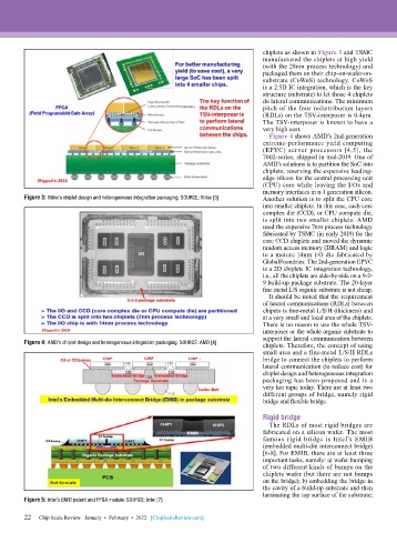
                                                                                Figure 4 shows AMD’s 2nd-generation
                                                                              extreme-performance yield computing
                                                                              (EPYC) server processors [4,5], the
                                                                              7002-series, shipped in mid-2019. One of
                                                                              AMD’s solutions is to partition the SoC into
                                                                              chiplets, reserving the expensive leading-
                                                                              edge silicon for the central processing unit
                                                                              (CPU) core while leaving the I/Os and
                                                                              memory interfaces in n-1 generation silicon.
        Figure 3: Xilinx’s chiplet design and heterogeneous integration packaging. SOURCE: Xilinx [3]  Another solution is to split the CPU core
                                                                              into smaller chiplets. In this case, each core
                                                                              complex die (CCD), or CPU compute die,
                                                                              is split into two smaller chiplets. AMD
                                                                              used the expensive 7nm process technology
                                                                              fabricated by TSMC (in early 2019) for the
                                                                              core CCD chiplets and moved the dynamic
                                                                              random access memory (DRAM) and logic
                                                                              to a mature 14nm I/O die fabricated by
                                                                              GlobalFoundries. The 2nd-generation EPYC
                                                                              is a 2D chiplets IC integration technology,
                                                                              i.e., all the chiplets are side-by-side on a 9-2-
                                                                              9 build-up package substrate. The 20-layer
                                                                              fine metal L/S organic substrate is not cheap.
                                                                                It should be noted that the requirement
                                                                              of lateral communications (RDLs) between
                                                                              chipets is fine-metal L/S/H (thickness) and
                                                                              at a very small and local area of the chiplets.
                                                                              There is no reason to use the whole TSV-
                                                                              interposer or the whole organic substrate to
                                                                              support the lateral communication between
        Figure 4: AMD’s chiplet design and heterogeneous integration packaging. SOURCE: AMD [4]   chiplets. Therefore, the concept of using
                                                                              small area and a fine-metal L/S/H RDLs
                                                                              bridge to connect the chiplets to perform
                                                                              lateral communication (to reduce cost) for
                                                                              chiplet design and heterogeneous integration
                                                                              packaging has been proposed and is a
                                                                              very hot topic today. There are at least two
                                                                              different groups of bridge, namely rigid
                                                                              bridge and flexible bridge.

                                                                              Rigid bridge
                                                                                The RDLs of most rigid bridges are
                                                                              fabricated on a silicon wafer. The most
                                                                              famous rigid bridge is Intel’s EMIB
                                                                              (embedded multi-die interconnect bridge)
                                                                              [6-8]. For EMIB, there are at least three
                                                                              important tasks, namely: a) wafer bumping
                                                                              of two different kinds of bumps on the
                                                                              chiplets wafer (but there are not bumps
                                                                              on the bridge); b) embedding the bridge in
                                                                              the cavity of a build-up substrate and then
                                                                              laminating the top surface of the substrate;
        Figure 5: Intel’s EMIB patent and FPGA module. SOURCE: Intel [7]

        22
        22   Chip Scale Review   January  •  February  •  2022   [ChipScaleReview.com]

