Page 22 - Chip Scale Review_January February_2022-digital
P. 22
Summary
                                                                                Heterogeneous package integration
                                                                              is going to be the main driver for
                                                                              semiconductor packaging in a variety of
                                                                              applications from system in package (SiP)
                                                                              to chiplet packaging. The main challenge
                                                                              for these expensive multi-chip packages
                                                                              remains how to keep assembly yield as
                                                                              high as possible so we can still enable
                                                                              the economic validity of Moore’s Law—
                                                                              even 50-plus years after the invention
                                                                              of integrated circuits. The chip bonding
                                                                              process is the center of IC packaging,
                                                                              including heterogeneous integration,
                                                                              where multi-chips are connected to each
                                                                              other for chiplet applications. Therefore,
                                                                              keeping chip attachment yield loss as
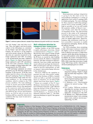
        Figure 7: Interference patterns detected to calculate PI layer thickness during wafer-level 3D bump measurement.  low as possible is necessary to enable
        over the bumps’ tops and chip area’s   Multi-reflectance detection for   heterogeneous packaging, thereby driving
        tops. Then, the highest and lowest points   transparent layer measurement  the industry forward.
        relative to the LSQ planes are calculated   Another feature of our WSI system   Our WSI technology shows promising
        for the bumps’ tops and chip area’s tops.   is multi-reflectance detection, which   results with respect to process control and
        Finally, the distances of the highest   is demonstrated in Figures 1 and 2.   the highest yield die bonding process—
        and lowest points along the LSQ planes   Measuring interconnect/bump height   both of which are necessary to enable these
        direction are separately measured as the   with respect to the RDLs underneath, e.g.,   expensive multi-chip advanced packages to
        bump coplanarity and CAW. According   the PI layer, is crucial for chip bonding   be successful products in the marketplace.
        to the measurement procedure explained   process control. PI, which is a transparent   In addition, the feature of transparent layer
        above, Figure 6a depicts interconnect/  material, and other transparent dielectric   detection and thickness measurement of
        bump coplanarity and CAW calculations   materials, have been widely used during   RDLs while inspecting interconnect height
        in the free-state condition. Figure 6b   recent advanced package development.   using WSI brings another dimension to
        shows examples of bump height and CAW   WSI can distinguish each layer of interest   advanced packaging process control.
        measurement by the WSI system.     based on process requirements, as well
          CAW and bump coplanarity are critical   as measure interconnect/bump reference   References
        parameters for the thermal compression   to the selected layer.         1.  P. Wesling, et al., “Heterogeneous
        bonding (TCB) process. TCB has been   Moreover, WSI has the capability to   integration roadmap, Chapter 8: Single
        widely used for silicon chip attachment   measure not only interconnect height,   chip and multi-chip integration,” IEEE
        during IC packaging. Figure 6a illustrates   but also the thickness of RDLs, beneath   2019 Ed.
        interconnect/bump shape under the free-  which are fully or partially transparent   2. S. Chitchian, “A deep-learning solution
        state condition, vs. the vacuum-state   layers so, therefore, we can detect light   for heterogeneous package inspection,”
        condition, which is related to the TCB   signals back from those layers. Figure   Chip Scale Review 24 (5), 2020.
        process condition. The main challenge   7 shows an example of the PI layer   3.  D. Malacara, et al., “Interferogram
        is how to assure successful bonding   thickness measurement during wafer-  analysis for optical testing,” CRC,
        conditions before silicon chip attachment   level 3D bump inspection. Light reflected   2005.
        to the expensive multi-chip package.   from the bottom of the PI layer has a   4.  K.G. Larkin, “Efficient nonlinear
        By measuring the described parameters   different thickness  compared  to the   algorithm for envelope detection in
        and defining the correct specification   real PI thickness, t PI , because of the PI   white light interferometry,” J. of the
        limits, we will be able to avoid chip   material’s refractive index, n PI . The WSI-  Optical Soc. of America A 13 (4), 1996.
        bonding yield loss caused by interconnect   measured thickness is equal to the optical   5.  M. Ishihara, et al., “High-speed surface
        conditions that may result in non-wet or   path, t PI ×n PI .             measurement using a non-scanning
        short bonding.                                                            multi-beam confocal microscope,”
                                                                                  Optical Eng. 38, 1999.


                       Biography
                         Shahab Chitchian is Chief Strategy Officer and R&D Corporate VP at INTEKPLUS CO., LTD., Daejeon,
                       South Korea. Previously, he was Senior Staff Process Engineer at Samsung Electronics, Semiconductor Test
                       and System Package division where he worked on advanced FOWLP development and high-bandwidth memory
                       packaging. He also was a Senior Process Engineer at Intel Co., Assembly and Test Technology Development
                       (ATTD), where he worked on EMIB package development. He received his MSc and PhD degrees in Electrical
                       and Optical Engineering, from the U. of North Carolina at Charlotte. Email shahab@intekplus.com


        20
        20   Chip Scale Review   January  •  February  •  2022   [ChipScaleReview.com]

