Page 59 - ChipScale_Mar-Apr_2021-digital
P. 59
Results and observations
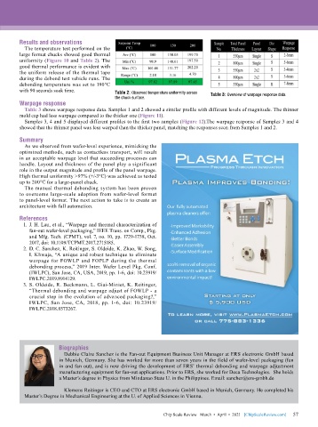
          The temperature test performed on the
        large format chucks showed good thermal
        uniformity (Figure 10 and Table 2). The
        good thermal performance is evident with
        the uniform release of the thermal tape
        during the debond test vehicle runs. The
        debonding temperature was set to 190°C
        with 90 seconds soak time.         Table 2: Observed temperature uniformity across
                                           the chuck surface.                 Table 3: Overview of warpage response data.
        Warpage response
          Table 3 shows warpage response data. Samples 1 and 2 showed a similar profile with different levels of magnitude. The thinner
        mold cap had less warpage compared to the thicker one (Figure 11).
          Samples 3, 4 and 5 displayed different profiles to the first two samples (Figure 12).The warpage response of Samples 3 and 4
        showed that the thinner panel was less warped than the thicker panel, matching the responses seen from Samples 1 and 2.

        Summary
          As we observed from wafer-level experience, mimicking the
        optimized methods, such as contactless transport, will result
        in an acceptable warpage level that succeeding processes can
        handle. Layout and thickness of the panel play a significant
        role in the output magnitude and profile of the panel warpage.
        High thermal uniformity >97% (+/-3°C) was achieved as tested
        up to 200°C for a large-panel chuck.
          The manual thermal debonding system has been proven
        to overcome large-scale adoption from wafer-level format
        to panel-level format. The next action to take is to create an
        architecture with full automation.

        References
          1.  J. H. Lau, et al., “Warpage and thermal characterization of
            fan-out wafer-level packaging,” IEEE Trans. on Comp., Pkg.
            and Mfg. Tech. (CPMT), vol. 7, no. 10, pp. 1729-1738, Oct.
            2017, doi: 10.1109/TCPMT.2017.2715185.
          2.  D. C. Sanchez, K. Reitinger, S. Oldeide, K. Zhao, W. Song,
            I. Khwaja, “A unique and robust technique to eliminate
            warpage for FOWLP and FOPLP during the thermal
            debonding process,” 2019 Inter. Wafer Level Pkg. Conf.
            (IWLPC), San Jose, CA, USA, 2019, pp. 1-6, doi: 10.23919/
            IWLPC.2019.8914129.
          3.  S. Oldeide, R. Beckmann, L. Giai-Miniet, K. Reitinger,
            “Thermal debonding and warpage adjust of FOWLP - a
            crucial step in the evolution of advanced packaging?,”
            IWLPC, San Jose, CA, 2018, pp. 1-6, doi: 10.23919/
            IWLPC.2018.8573267.


                       Biographies
                         Debbie Claire Sanchez is the Fan-out Equipment Business Unit Manager at ERS electronic GmbH based
                       in Munich, Germany. She has worked for more than seven years in the field of wafer-level packaging (fan
                       in and fan out), and is now driving the development of ERS’ thermal debonding and warpage adjustment
                       manufacturing equipment for fan-out applications. Prior to ERS, she worked for Deca Technologies.  She holds
                       a Master’s degree in Physics from Mindanao State U. in the Philippines. Email: sanchez@ers-gmbh.de

                         Klemens Reitinger is CEO and CTO at ERS electronic GmbH based in Munich, Germany. He completed his
          Master’s Degree in Mechanical Engineering at the U. of Applied Sciences in Vienna.


                                                                                                             57
                                                             Chip Scale Review   March  •  April  •  2021   [ChipScaleReview.com]  57

