Page 7 - ChipScale_May-June_2020-digital
P. 7
TECHNOLOGY TRENDS


                           A new era of smart packaging:


                           the introduction of chiplets


                           By E. Jan Vardaman [TechSearch International, Inc.]
        T        he use of chiplets will be   AMD                             functions such as a modem. The active


                 one of the most important
                                                                              interposer can contain active parts
                                             AMD’s current chiplet solution uses
                 developments for the next 10
                                                                              controller hub (PCH) that manages
                 to 20 years, according to Dr.   a laminate substrate. The company has   of the system, such as the platform
                                           shipped multiple versions of its server
        Douglas Yu, TSMC’s Vice President,   processor using chiplets. Up to eight 8-core   I/O for the system. The active interposer
        Research & Development/Integrated   processors are tightly coupled together on   is mounted on a package substrate with
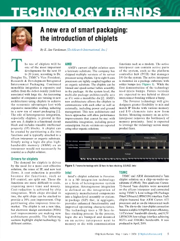
        Interconnect Packaging. Continued   an organic substrate. The chiplets can be   solder bumps (see Figure 1).  While the
        monolithic integration is expensive and   binned and speed-sorted before assembly   first demonstration of the technology
        suffers from the defect density yield loss   in the package. At the system level, the   used micro bumps. Future versions
        associated with large die. An increasing   multi-die package architecturally acts   are expected to use hybrid or direct
        number of companies are turning to new   as if it were a monolithic die [2]. AMD’s   interconnect bonding without a bump.
        architectures using chiplets to achieve   new architecture allows the chiplets to    The Foveros technology will give
        the economic advantages lost with   communicate with each other as well as   designers greater flexibility to mix and
        expensive monolithic scaling, ushering   externally, including power and ground   match IP blocks with various memory
        in a new era of smart packaging [1].   management. This new architecture and   and I /O elements i nto new for m
        The role of heterogeneous integration,   future approaches will allow performance   factors. Mounting memory on an active
        especially chiplets, is pivotal in this   improvements that cannot be met with   interposer removes the bottleneck of
        new era. A chiplet is a functional circuit   monolithic integration, including power   memory proximity.  Intel is expected
        block and includes reusable intellectual   consumption. Future versions are expected   to leverage the technology across many
 When Moore’s Law no longer gets your   property (IP) blocks. A chiplet can   using other organic solutions.  product lines.
        be created by partitioning a die into
        functions and is typically attached to a
 ICs where they need to go.  silicon interposer or organic substrate.
        Simply using a logic die plus high-
        bandwidth memor y (HBM) on an
 FormFactor takes on the challenge with test    interposer would not necessarily be
 and measurement solutions to reduce the   counted as a chiplet solution.
 manufacturing cost of advanced packages.  Drivers for chiplets
          The demand for chiplets is driven
 Advanced packaging adds a new vertical dimension to IC layout. Multiple   by the need for a more cost-effective   Figure 1: Foveros technology with 3D face-to-face stacking. SOURCE: Intel
 dies merge into single systems with unprecedented interconnect density.   solution, the reuse of IP, and new test
 Performance goes up. Power consumption goes down.   f lows. A cost reduction is possible   Intel  TSMC
        b e c a u s e d ie f u n c t io n s , s u c h a s    Intel’s chiplet solution is Foveros.   TSMC and ARM demonstrated a 7nm
 And wafer-level test and measurement becomes nearly essential to   I/O control, are split out. These die   It is a 3D integration technology   chiplet solution on a chip-on-wafer-on-
 guarantee cost-effective fabrication and packaging. Successful verification   functions are more difficult to scale,   as a form of heterogeneous system   substrate (CoWoS). Two quad-core Cortex-
 at this level requires probing and measuring with extraordinary precision,   requir ing more time and money.   integration. Heterogeneous integration   72-based 7nm chiplets were mounted
 optically, electrically and mechanically.  Cost reduction is achieved by chip   is def i ned a s t he i nt eg r at ion of   on the silicon interposer and connected
        integration.  With chips  divided in   separately manufactured components   using TSMC’s Low-voltage-IN-Package
 FormFactor not only understands the problem, it’s also providing timely   two, the split chips can be stacked to   into a higher-level assembly or system-  INterCONnect (LIPINCON) interface. Each
 solutions to advance yield knowledge at every phase of wafer level test in   provide a 20% cost improvement. Chip   in-package (SiP) that, in aggregate,   chiplet featured four ARM Cortex A72
 advanced IC packaging.  partitioning also improves time-to-  provides enhanced functionality and   processors and an on-die interconnect mesh
        market.  The chiplet is not a new idea,   improved operating characteristics.   bus. The die-to-die inter-chiplet connection
 Let us help you rise to the occasion. Visit www.formfactor.com/go/ap.  but electronic design automation (EDA)   The technology uses a 3D face-to-  features scalable 0.56pJ/bit power efficiency,
        tool improvements are making new   face stacking process. In the process,   1.6Tb/s/mm  bandwidth density, and 0.3V
                                                                                        2
        architectures possible. The following   logic die are bumped and  mounted   LIPINCON low-voltage interface achieving
        sections highlight chiplet technology by   on  a n  a c t ive  i nt e r p o se r  nex t  t o   8GT/s and 320GB/s bandwidth. It was
        different entities.                memory or die with communication   produced in April, 2019.


                                                               Chip Scale Review   May  •  June  •  2020   [ChipScaleReview.com]  5 5


 FF_Adv_Packaging_ChipScale_Review.indd   1  5/4/20   12:35 PM

